Author Archives: insights-from-leading-edge

Economy Threatens Semi Growth, not Technology – so Say Fab Engineers at ASMC

It’s still spring in the north-eastern part of North America, and that means it’s the time of year for the Advanced Semiconductor Manufacturing Conference, in the amiable ambiance of Saratoga Springs, New York. The conference took place last month, on May 13 – 16.

As the name says, ASMC is an annual conference focused on the manufacturing of semiconductor devices; in this it differs from other conferences, since the emphasis is on what goes on in the wafer fab, not the R&D labs, and the papers are not research papers. After all, it’s the nitty-gritty of manufacturing in the fab that gets the chips out of the door, and this meeting discusses the work that pushes the yield and volumes up and keeps them there.

I always come away impressed by the quality of the engineering involved; not being a fab person myself any more, it’s easy to get disconnected from the density of effort required to equip a fab, keep it running and bring new products/processes into production. Usually the guys in the fab only get publicity if something goes wrong!

There were 81 papers spread over the three days, with keynotes from Subi Kengeri of GLOBALFOUNDRIES, Vivek Singh and Tim Hendry of Intel, and Bill McClean of IC Insights, and also a panel discussion on the benefits/pitfalls of 450mm wafers. This latter is particularly apposite here in Saratoga Springs since we have the Global 450 Consortium building their new fab at CNSE in Albany, just down the road from here.

The conference kicked off with Subi Kengeri’s keynote – “Assessing the Threats to Semiconductor Growth: Technology Limitations versus Economic Realities” – essentially, will Moore’s law run out of steam before or after chips get too expensive to sell?
??????

Subi Kengeri of GLOBALFDOUNDRIES giving the opening keynote at ASMC

On the one hand, we anticipate huge growth in revenue on the back of the mobile industry, with the foundries expected to outpace the overall industry, and leading-edge revenue doubling in the next five years:

And we know that technologically we can get to 14nm or even 10nm with multiple patterning, finFETs, etc., and possibly new materials.

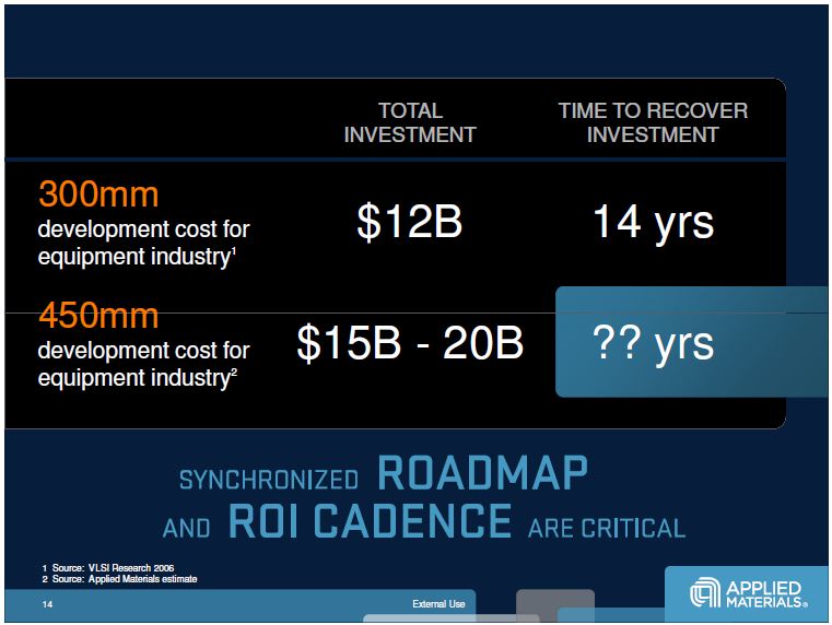
On the other hand, SoC designs are getting larger, faster, and more complex, and wafer fab costs are going up, with lithography being the biggest component. (It’s worth noting here that at the 20nm generation, the middle-of line (MOL) processing separates from the back-end of line (BEOL), since the 1X interconnect level has to be double-patterned.)

This increased design and fab complexity also adds to development time and increases the time-to-volume (TTV), adding a time cost and reducing the return on investment.  This could conceivably get the industry into a feedback loop, since TTV delay slows down industry growth, which slows downs investment, which slows down development, which slows down TTV.

The other obvious effect is the industry consolidation which we’ve all been part of – according to Subi only four companies will be fabbing at the 14nm node:

I had wondered why IBM wasn’t on the list until I saw the 50K wafers/month cut-off; even with all the games chips that IBM has churned out over the last few years, I doubt that IBM has hit that number.

If the predictions are correct, by 2016 28nm and below will make up 60 percent of the foundry market, split between four companies (or three, if Intel’s foundry ambitions don’t work out). That thought raised the prospect of capacity limitations, and gave Subi a chance to promote GLOBALFOUNDRIES as the only one of the three with a global footprint, and not in geographically or politically risky zones. 

He finished his talk by identifying critical growth enablers for the industry as optimized SoC technology architecture (with a focus on techno-economics), coupled with true collaborative R&D, and of course the global footprint. And he also asked all of us in the room which was the biggest threat to growth – technology scaling limits, or the economic realities? Being techies, we all know that the next few generations are within sight technically, so we all voted for the economic problems – the part we can’t control!
???

The final vote

As you can see, the vote was pretty overwhelming.

N.B.  All images courtesy of GLOBALFOUNDRIES.

Intel Foundries MEMS for Fuel Cell Start-up Nectar

In the last couple of years there have been announcements that Intel will be acting as a foundry for FPGA company Achronix, PLD maker Tabula and programmable network processor provider Netronome, as well as much speculation about making chips for Apple.

All these reports refer to using Intel’s leading-edge 22-nm tri-gate process. However, at CES a couple of weeks ago, my eye was caught by a 200-mm wafer on display at the booth of a little company called Nectar, who were pitching their fuel-cell based USB charging system. They claim that the charger can top up an iPhone battery at least ten times before the fuel pod has to be changed. The whole device can be held in one hand:


Fig. 1 Nectar fuel-cell charger (at right) on display at CES
The cell uses butane fuel in a silicon-based power cell, and by the look of the image below the cells are ~22 mm square.

Fig. 2 Nectar MEMS wafer on display at CES

The press pack given out at the show includes a paper [1] with a description of the technology; a solid oxide fuel cell (SOFC) is used, which is compatible with silicon processing. I’m not a fuel cell expert, so to quote from the paper:

"Fuel cells operate by creating opposing gradients of chemical concentration and electrical potential. When an ion diffuses due to the concentration gradient, the associated charges are transported against the electric field, generating electrical power. In the case of SOFCs, the mobile ion is O2-, and the oxygen gradient is created by providing air on one side (the cathode) and a fuel mixture which consumes any free oxygen on the other side (the anode). Any fuel which burns oxygen will produce power in an SOFC." The schematic below (Fig. 3) illustrates the process.


Fig. 3 Operating principle of solid oxide fuel cell

The butane has to be cracked so that hydrogen is available, which is done in a "fuel processor" within the cell. The following diagram shows the sequence of power generation [1].


Fig. 4 Diagram of fuel cell power generator

The Nectar generator chip contains the fuel processor, fuel cell stack, and catalytic converter. The fuel processor cracks the butane into hydrogen and carbon monoxide by using a lean mixture of air and butane to give incomplete combustion; then O2- ions from the air feed on the other side of the SOFC stack migrate through the stack and combine to give water and carbon dioxide; then the exhaust gases exit through a catalytic converter.

It is here that the MEMS structure comes in – even incomplete combustion of the butane gives temperatures of 600 – 800C, so to integrate this into a package that can be carried around, and also must have conventional silicon for power conditioning has to be a challenge. The fuel processor uses a mechanically suspended reaction zone formed in silicon, with a heat exchanger adjacent to the reaction zone, as shown in Fig. 5 [1, 2]:


Fig. 5 Experimental (top) and later (bottom) MEMS fuel processor

The nitride tubes contain the gas stream, while the silicon bars provide the heat transfer from the exit stream to the input stream. Fig. 6 shows the modeled heat transfer in a pair of tubes (red = hot, blue = cool) [1]. The U-bend at the end is the reaction zone; ignition is started using a platinum heater deposited on the surface, and once started continues autothermally.


Fig. 6 Schematic of modeled heat recovery in reaction loop

The SOFC itself is built of yttrium-stabilized zirconium oxide (YSZ) plates held in a nitride matrix, supported on silicon walls. In order to keep the profile as slim as possible a "planar stack" of plates is formed as shown schematically in Fig. 7(a), with the detail of a single plate in Fig 7(b)[1].


Fig. 7 (a) Schematic of SOFC plates and (b) Cross-section of single cell

Details of the anode and cathode materials are not given, but they clearly have to be porous to allow the gases to diffuse through and react. Similarly nothing is said about the catalytic converter, but that also should be compatible with MEMS manufacturing.

The inherent ability of MEMS processes to provide vacuum-sealed structures helps contain the heat generated within the system, and the chamber is lined with reflective shielding to further reduce heat losses. Even so a new sealing glass had to be developed, since the conventional lead-glass frits used in many MEMS devices was not up to the job.

The whole assembly is packaged in a “tin can” with the gas inlets and exits on the reverse side of the package:


Fig. 8 Assembled and packaged Nectar fuel cell

Of course, smart as the fuel cell manufacturing is, it is only part of a charging system. Fig 9 [1] is a block diagram of the whole system, showing the peripheral components needed to complete the unit and turn it from a concept into a functioning charger. The battery allows power to be drawn instantaneously from the charger while the fuel cell fires up, and also powers the supporting components. 

Fig. 9 Block diagram of Nectar fuel-cell charging system

I started this blog off by talking about Intel, then veered off into a description of the Nectar charger – what was I babbling about? Well, when I was looking at the charger at CES I had a word with Sam Schaevitz of Lilliputian Systems, which developed the Nectar, and asked him who made the MEMS, expecting to hear about of one of the MEMS foundries that are around. (Lilliputian is a spin-off of MIT – Sam is founder and CTO.)

Much to my surprise, he answered "Intel"! As I said at the beginning, there has been quite a bit of comment about Intel moving to the foundry model, but nothing about them being in the MEMS business. It turns out that the work is done at Intel’s fab in Hudson, Mass., which those with long memories will recall was the DEC fab bought by Intel when DEC went under back in 1998.

I had assumed that it would have been closed long ago, but Intel claims to have put $2B into the plant, converting it to 130 nm back in 2001, and it’s now known as Fab 17. It is now Intel’s sole remaining 200 mm facility. In addition they have their Massachusetts Microprocessor Design Center and the Massachusetts Validation Center on the same site, employing ~1700 in total.


Fig. 10 Intel’s Fab 17 in Hudson, MA (source: Intel)

Intel’s Global Manufacturing Fact Sheet states that the fab manufactures “chipsets and other” – the Nectar chip is clearly an “other”! Nectar announced their supply link with Intel back at the end of 2010, but I missed it at the time; Intel Capital also has a stake in Lilliputian.

Aside from the regular processing equipment, Intel must have invested in deep RIE etchers, never mind the deposition gear capable of forming YSZ and the other exotic materials likely used for the anode/cathode and catalytic converter. Presumably Intel’s need for 130-nm chipsets is slowly fading; this looks like a praiseworthy way of keeping the fab going, as well as supporting a local start-up – and one wonders what other foundry work is going on there. If you do have the urge to buy a Nectar mobile power system, it will be available through Brookstone in the summer.

References:

[1] S. Schaevitz, Powering the wireless world with MEMS, Proc. SPIE 8248, Micromachining and Microfabrication Process Technology XVII, 824802 (February 9, 2012)

[2] L. Arana et al., A Microfabricated Suspended-Tube Chemical Reactor for Thermally Efficient Fuel Processing, J. MEMS 12(5) 600-612

IBM surprises with 22nm details at IEDM

Monday afternoon at the 2012 IEEE International Electron Devices Meeting, IBM discussed their 22nm SOI high-performance technology [1], aimed at servers and high-end SoC products. To an extent, this is an extension of the 32nm process, using epitaxial SiGe for the PMOS channels and stress, and dual-stress liners for both NMOS and PMOS strain. However, there were a couple of surprises buried in there — at least for me!

The first surprise was that this is a gate-first process, contrary to the announcements made by the Common Platform group that the 20nm class processes would be gate-last. The difference seems to be that this technology IS aimed at high performance servers and their support devices, not consumer products, and this is IBM’s process for its high-end products, so they are sticking with the proven formula and pushing it to the next level.

The gate dielectric stack has been scaled to reduce the inversion thickness (tinv) by 7%/10% (NMOS/PMOS), without affecting mobility, modifying the clean, depositions (using ALD for the interfacial oxide), and anneal steps to achieve the lowest tinv published so far, and reducing DIBL by 6%/8%.

The second surprise was that e-Si:C (embedded carbon-doped source/drains) has been used for NMOS stress — IBM claimed that this is the first time in a production process. I had just about written e-Si:C off as a viable manufacturing technique, since I’ve been hearing over the last few years that the carbon is not stable and does not stay in the substitutional crystalline sites where it’s needed. However, here we are told that it is stable and that it survives all the backend processing, even with the 15 layers of metal used in this technology.

Fig. 1: TEM cross-sections of e-SiGe in PFET (left), and e-Si:C in NFET [1]

The e-Si:C incorporates ~1.5% C, which combined with fourth-generation e-SiGe with more Ge and the dual-nitride stress liners, gives 25% more strain than the 32nm process.

The gate-first approach allows conventional contacts and self-aligned silicide, and judging by Fig. 3, raised source/drains help to reduce S/D resistance and keep the gate/contact capacitance under control.

The embedded trench DRAM is not a surprise, IBM has a long history in the field and they have now brought it to the point where access time is shorter than SRAM [2, 3, 4].

Fig. 2: IBM roadmap for e-DRAM [2]

The big change here is that the substrate wafer has an N+ epi layer on it to replace the diffused cell plate of earlier generations. This allows denser packing, since a formerly-needed diffused spacer is removed, giving a cell size of 0.026 μm2. It also enables deeper trenches, giving higher cell capacitance for an areal capacitance of 280 fF/ μm2. The trench capacitors are also used as decoupling capacitors, and these are isolated by deep trench isolation so that they can be biased independently.

Fig. 3: (left) SEM cross-section of e-DRAM trench capacitors; (right) plan-view and
cross-section schematics of decoupling and isolation trenches, showing N+ epi plate
[1]

(As an aside, one of the comments from Greg Taylor of Intel in his microprocessor talk in Sunday’s IEDM short course was that the analog functions that are part of a CPU are getting more significant as dimensions shrink. Both Intel and IBM are now using on-chip decoupling capacitors; Intel with MIMCAPs, and IBM with trench capacitors.)

The complexity of IBM’s server chips is reflected in the 15 levels of metal. The first level is doubled-masked with a litho-litho-etch sequence to allow for orthogonal layout; the rest are single-patterned using uni-directional layout. Self-aligned vias help with packing, and both ultralow-k and low-k dielectrics are used as needed.

IBM is prototyping 22nm server parts right now, but even when they get into the servers for sale, I likely won’t get my hands on one — a bit beyond my procurement budget!

[1] S. Narasimha, IEDM 2012 pp. 52-55
[2] S. Iyer, ASMC 2012
[3] N. Butt, et al., IEDM 2010 pp. 616-619
[4] J.Bart et al, IEEE Journal of Solid-State Circuit, Jan 2011

Intel details 22nm trigate SoC process at IEDM

After launching their 22nm tri-gate high-performance logic product back in the spring, Intel have been promising to show off their SoC derivative, and yesterday was the day at the 2012 IEEE International Electron Devices Meeting. [1]

As you can see from Table 1, we now have six transistor options; the high-voltage transistors use a thicker gate dielectric stack (Fig. 1), and the gate pitch and gate lengths have been tuned to suit the end purpose, and of course there is some (unspecified) source/drain engineering.

Intel 22nm SoC transistor options [1]

Fig. 1: TEM linear- and cross-sections of, and tilted SEM of,
logic (top) and high-voltage (bottom) transistors
[1]

If I read the paper correctly, the SoC process can incorporate up to twelve metal layers, with up to six 1�? layers, and an extra 3�? level, but only one 4�? level Fig. 2). When it comes to the passives, the same MIMCAP layer is used as we saw in the CPU together with similar finger capacitors to the 32nm SoC; inductors are also formed in the 6μm thick top metal; and there are precision resistors available.

Fig. 2: Interconnect stacks for CPU (left) and SoC processes [1]

A bunch of SRAM cells are offered, both six- and eight-transistor varieties, with the 6T cells ranging from the minimal 0.092 to 0.13 μm2. These show the quantization of the transistor size quite nicely — if you look closely at Fig. 3, you can see that the number of fins used for each transistor increases with the size of cell, with the exception of the T3 and T4 PMOS pull-up devices, which only have one fin.

Fig. 3: Intel’s 6T SRAM options in their SoC technology, including
high density / low leakage (HDC), low voltage (LVC), and high performance (HPC)
[1]

Overall Intel claims a 100-200 mV reduction in Vt for all transistor types, leading to a ~40% reduction in dynamic power.

Intel is trying to catch their SoC schedule up with the CPU launches, so we will likely see 22nm SoC chips next year, and the 14nm CPU and SOC processes should be launched in parallel, theoretically by the end of 2013.

[1] C-H Jan, IEDM 2012 pp. 44-47

GlobalFoundries takes on Intel with 14nm finFET “eXtreme Mobility” process

A week after Intel were claiming that their 14nm process will be ready to go at the end of next year, GLOBALFOUNDRIES (GF) announced that they will have a 14nm finFET process for launch in 2014. Unfortunately they timed it to coincide with the iPhone 5, so we at Chipworks were tied up for a few days tearing it down.

However, I don’t want to ignore this development — it could make the 2014 an interesting year! GF have dubbed the new process 14XM, for "eXtreme Mobility," since from the start it has been targeted on mobile applications — after all, mobile products are the volume driver in the chip business these days.

And what’s the biggest complaint from mobile users? Having to charge them so often, as battery technology has not improved at anything like a rate comparable to chip performance.

So while GloFo got started in high-k metal-gate (HKMG) making 32nm parts for AMD, they have seen the obvious and are generating low-power processes, beginning with the 28-SLP, moving to the 20-LPM, and now the 14XM.

The 20-LPM process claims a 40% reduction in power from the 28nm generation, and the 14XM claims 40%-60% increased battery life over 20-LPM. The 20nm generation is scheduled for next year, and as noted earlier 14XM is due out in 2014, a year later, breaking the two-year cadence that we’ve all got used to. Apparently 20nm wafers are running the full process in the Malta, NY fab right now.

They’re accelerating the process launch by using the 20-LPM middle/back end-of-line metal stack with the finFET front end. In the 20nm process the 1x metal pitch is 64nm and the single-patterned metal is 80nm — coincidentally, the latter is the same as Intel’s tightest pitch in their 22nm product.

20nm metal pitches shown at the 2012 Common Platform Tech Forum (CPFT)

The use of the 3D finFET structure enables a higher performance/unit area, or lower power/unit area at a given performance at the transistor level. The graph below shows some estimates made by their R&D group.

SoC Performance vs. power — lower power at constant frequency [1]

Functional scaling itself will be limited to some extent by the 20-LPM metal density, but presumably some die shrink can be achieved by using more metal layers, and also the increased current density will allow some compaction since higher-current transistors will be smaller. Keeping single patterning will mitigate the cost, compared with double patterning for denser layers.

The process will also continue from the 20-LPM process in that it will use gate-last (replacement metal gate) technology on a bulk substrate. The R&D group in New York has published a couple of papers [2, 3] referencing a 40nm fin pitch, but 14XM will have a fin pitch of 48nm to leave some slack in the lithographic challenge, and minimize quantization errors. Together with the metal pitches of 64 and 80nm, it implies a 16nm grid as a basis for layout. The use of 64nm Metal 1 presumably also means that the contacted gate (CG) pitch will be 64nm.

The Intel 22nm process has a fin pitch of 60nm, and a CG pitch of 90nm, so it’s not unreasonable to assume that their 14nm process will have similar numbers.

We will see whether the fin will be tapered similar to Intel’s; these images (below) from CPTF seem to show a vertical fin atop the STI profile, but then, they are only schematics. Using a single (STI) etch to shape the fins (as I think Intel does) should certainly be less complex than trying to get vertical-walled fins on top of the STI trench sidewall.

The economic challenge in going to 14nm is almost as huge as the technical challenge, and keeping the cost/power/performance (CPP) metric in check as process complexity spirals upwards has caused inevitable concern. In particular, the cost benefits of shrinking die size tends to go away as the lithography demands double, triple, and even quadruple patterning.

Jen-Hsun Huang of Nvidia has publicized his concern about increasing wafer costs at last year’s IPTC (International Trade Partner Conference) meeting — the plot below shows the increasing gap in wafer cost between successive nodes:

So if GLOBALFOUNDRIES, or any other foundry, wants to keep the customers coming, they have to mitigate the cost increase going to the next node. Taking a hybrid approach such as the 14XM process should be an attractive option for their existing and future customers.

It’s interesting to note that TSMC has changed tack slightly and are now saying that they will be using finFETs at 16nm, not 14nm. They are also claiming that their 20nm metal pitch is leading-edge at 64nm, although that’s the same as GF’s. It’s tempting to wonder if TSMC will also use a hybrid approach and transfer their 20nm back-end to the 16nm node, since the arguments are the same. Chenming Hu thinks so, anyway. TSMC are predicting 16nm risk production in 2014.

We’ll see if GF can match Intel’s timing — Mark Bohr sounded very confident at the Intel Developer Forum, when he said their 14nm product would be ready for the tail end of next year. Will we have GF-produced finFETs in early 2014? And will their finFETs be better than Intel’s?

My thanks to Subi Kengeri for clearing up some of the technical details.

[1] A. Keshavarzi et al., Architecting Advanced Technologies for 14nm and Beyond with 3D FinFET Transistors for the Future SoC Applications, Proc. IEDM 2012, pp. 67-70.

[2] T. Yamashita et al., Sub-25nm FinFET with Advanced Fin Formation and Short Channel Effect Engineering, Proc. VLSI 2011, pp. 14-15.

[3] C.-H. Lin et al., Channel Doping Impact on FinFETs for 22nm and Beyond, Proc. VLSI 2012, pp. 15-16.

The Elephant Has Left the Room – 450 mm is a Go!

It’s the day before Semicon opens up, and we have had a slew of announcements on 450 mm, the biggest of which was the joint ASML/Intel notice that Intel will be taking a share of ASML as a way of funding 450 mm and EUV R&D. Simultaneously imec released that the Flemish government would invest in their upcoming 450-mm facility, and imec and KLA-Tencor declared that a 450-mm capable SP3 450 unpatterned wafer defect inspection tool had been installed at imec.

ASML announced it as a “co-investment program” in which Intel would invest EUR829 million (about $1B) over the next five years, EUR553M of which would be in 450 mm R and D. Intel focused more on the R and D and described the financial details later.

They cited the classic economics of doubling the wafer size, and the potential die cost reduction:

All of which is logical, but ASML has been notably reticent about making any comments on 450-mm R and D in the past, to the point where some industry watchers (including me) have wondered if we would ever get there; if the biggest litho vendor isn’t on board, there won’t be any 450-mm fabs even if all the other equipment companies are ready.

Which brings me to the elephant in the title. Last year at Semicon there was a 450 mm panel, and everyone was pontificating wisely, until Bob Johnson of Gartner commented on "the elephant in the room – ASML has no 450-mm program, so why are we bothering to even talk about it?" (my paraphrasing). Which kind of shut the whole thing down.

However, that particular pachyderm has clearly moved on, and we have an ASML roadmap with both 450 mm and EUV in it:

We won’t have any production tools until 2018, but at least a huge barrier to adoption is lifted; now there are just the simple engineering tasks of getting a substrate the size of a turkey platter exposed with patterns with feature sizes of 14nm or smaller. Has anyone said that this industry is crazy?

By coincidence Mike Splinter of Applied Materials was speaking at the imec Technology Forum, and he commented that 300-mm had just about paid off its development costs as of now, roughly 14 years after the launch of the first systems. He guesstimated the costs for developing 450 mm as $15 – 20B, with an as yet unknown payoff time. (Has anyone said that this industry is crazy?) However,  he also said this time last year that Applied would spend over $100M on 450 mm and that "450 mm is going to happen."

Clearly Intel has recognised that if it wants 450 mm to go forward, then it has to pony up some cash to encourage the litho side, and it is already invested in the consortium being set up at Albany. For anyone interested in the financial side of the deal, check out the press releases linked above, or watch ASML CFO Peter Wennink in a video.

Looks like 450 mm is actually going to happen!

Sony’s PS Vita Uses Chip-on-Chip SiP – 3D, but not 3D

At the tail end of last year Sony released their PlayStation Vita, and it was duly torn down by iFixit and others. In due course we took it apart too, though we didn’t post it on our teardown blog.

Sony CXD5315GG in the PlaySation Vita

Inside we found the usual set of wireless chips, motion sensors, and memory, but the key to the increased performance of the PS Vita is the Sony CXD5315GG processor, a quad-core ARM Cortex-A9 device with an embedded Imagination SGX543MP4+ quad-core GPU.

Above I said that we found memory, but actually the only discrete memory that we found on the motherboard was 4 GB of Toshiba flash; and Sony’s specification states that there is 512 MB (4 Gb) regular RAM, plus 128 MB (1 Gb) VRAM (video RAM). In a phone that would tell me that there is memory in a package-on-package (PoP) configuration, mobile SDRAM in the top part and the processor in the bottom part.

However, when we took the part off the board and did a set of x-rays, the side view proved me wrong – it’s a stack, and the close-up shows that there appear to be five dies in there, a thick die at the base, a thinner one immediately on top and three smaller die on top of that. The second die down could be a spacer, since there don’t seem to bond wires going to it.

Side x-ray images of Sony CXD5315GG

This immediately led us to speculate – if the second die up is the VRAM, is it wide I/O DRAM, and is it using through-silicon vias (TSVs)? Time for a real cross-section to check that out, and almost predictably we were disappointed:

Sony CXD5315GG package cross-sectioned

This type of face-to-face connection showed up back in 2006 in the original Sony PSP, and Toshiba had dubbed it “semi-embedded DRAM”, now they are calling it “Stacked Chip SoC”. The ball pitch is an impressive ~45 µm, almost as tight as TI’s copper pillars, but they are staggered to achieve 40-µm pitch.

So what are the five chips that are in the stack? At the base we have the processor chip; face to face with it is a Samsung 1-Gb wide I/O SDRAM; and the top three dies comprise two Samsung 2-Gb mobile DDR2 SDRAMs, separated by a spacer die, and conventionally wire-bonded. The base die is ~250 µm thick, and the others ~100 – 120 µm.

When we look at the die photos of the processor and the 1-Gb memory, we can see that they are purposely laid out for the stacked-chip configuration, since in the centres of both is an array of matching bond pads.

Die photos of the Sony CXD5315GG (left) and Samsung 1-Gb wide I/O SDRAM with bond pad arrays annotated

Close examination reveals that there are 1080 pads in two blocks of 540 (2 sub-blocks of 45 rows of 6 pads), so likely 2 x 512 bit I/O operation, possibly sub-divided into 4 x 128.

Wide I/O bond pad arrays in Sony CXD5315GG (top) and Samsung SDRAM

Last year at ISSCC Samsung described a similar wide I/O DRAM using TSVs [1], claiming a data bandwidth of 12.8 Gb/s, four times the bandwidth of an equivalent LPDDR2 part. I doubt that the authors expected their design to be in a volume consumer device before the end of the year, but that seems to be what happened!

Chip architecture of Samsung 1Gb Wide-I/O DRAM and SEM image of microbumps (Source: Samsung/ISSCC)

This uses similar I/Os, but not the same as, the JEDEC wide I/O standard issued earlier this year (which calls for 50 rows of 6 pads in each block), and of course it predates it by about a year.

By combining the processor with the different memories in the same package in the Vita, Sony and Toshiba have produced one of the few true system-in-package (SiP) parts that we have seen. And I would call it 3D, even though industry convention is now restricting that term to TSV-based parts – so it’s not 3D, in our current argot.
In a way this device highlights the commercial barriers to introducing TSVs into the SiP world, since not only do the corresponding parts have to be designed to suit the I/Os, but at least for a two-stack the technology is already there; so the performance cost/benefit has to be critical enough to require TSVs for that third and more die. Admittedly the demands on mobile devices are increasing at an astounding pace, but it still seems a while before we’ll see TSVs in commercial devices. Time will tell!

[1] J-S. Kim et al., A 1.2V 12.8GB/s 2Gb Mobile Wide-I/O DRAM with 4Ã??128 I/Os Using TSV-Based Stacking, ISSCC 2011, pp. 496 – 498.

Intel’s 22-nm Trigate Transistors Exposed

Last week Intel had their Q1 conference call for financial analysts, and revealed that the 22-nm Ivy Bridge parts would make up 25% of their shipment volume in the second quarter of this year.  That means that a good quantity will already will have shipped, and we managed to track some down in Hong Kong a few weeks ago.  Of course we got in touch ASAP and the parts duly arrived, and they were the real thing.

Fig. 1 Intel Xeon E3-1230V2 Server CPU

We obtained samples of Xeon E3-1230 v2 CPUs, which are four-core, 3.3 GHz, 64-bit parts intended for the server market. Here is a die photo of the transistor level, with annotations from Intel’s Ivy Bridge launch yesterday:

Fig.2 Intel Xeon E3-1230V2 Die

A quick cross-section reveals that Intel have stayed with the nine metal layers used in the last two generations:

Fig. 3 Intel Xeon E3-130V2 General Structure

A closer TEM image (Fig. 4) shows the lower metal stack and a pair of multi-fin NMOS and PMOS transistors. This section is parallel to the gate, across the fins, and we can see the contact trenches and metal levels M1 up to M5.

We have to digress here a little to explain what we’re looking at.  A typical TEM sample is 80 – 100 nm thick, to be thin enough to be transparent to the electron beam and at the same time have enough physical rigidity so that it does not bend or fall apart.

Here we are trying to image structures in a die with a gate length of less than 30 nm; so if we make a sample parallel to the gate, and if the sample is aligned perfectly along the centre of the gate, then it will contain the gate plus at least part of the source/drain (S/D) silicon and contacts on either side.

Fig. 4 TEM Image of Lower Metals and NMOS and PMOS (right) Transistors

That is what we see above – I have labeled the gate and contact stripes, and we have PMOS on the right and NMOS on the left.  The tungsten-filled contacts obscure parts of the gate, but we can clearly see that the PMOS S/D fins have epitaxial growth on them, and the fins have an unexpected slope – a little different from Intel’s tri-gate schematic shown last year –see Fig.5.

Fig. 5 Intel Schematic of Tri-Gate Transistor

If we zoom in a bit further into the PMOS gate (Fig. 6), we can see how the gate wraps over the fin, and the rounded top of the fin.  The thin dark line adjacent to the fin is the high-k layer and just above that is a mottled TiN layer that is likely the PMOS work-function material, as in the 32-nm and 45-nm parts.

Fig. 6 TEM Image of PMOS Gate and Fin Structure

Fig. 7 shows a section of an NMOS transistor.  There is a ‘ghost’ of the contact behind the gate, but the gate structure itself looks similar to the PMOS, with the exception of the work-function material just above the high-k layer (as expected).

Fig. 7 TEM Image of NMOS Gate and Fin Structure

Fig. 8 gives me an opportunity to show off our new TEM – we have recently purchased an FEI Osiris machine, which upgrades our capability considerably. Here we have a lattice image of a fin in an NMOS transistor; the diamond-like layout of the pattern of dots is actually created by the columns of atoms in the silicon crystal lattice. This tells us that the sample is oriented in the <110> direction, which given that silicon has a face-centred cubic structure in which equivalent planes are at right angles, means that the channel direction is also <110>.

Fig. 8 TEM Lattice Image of NMOS Fin Structure

To fully understand what we’re looking at, of course, we need to see what’s happening in the orthogonal direction, along the fin and cross-sectioning the gate – as in Fig. 9. This shows an array of PMOS transistors over a single fin, four functional gates and two dummy gates at the ends of the fin. Again the TEM sample is thick compared with the feature size, so we are seeing the gate on the side(s) of the fin, not just the top. The fin ends have the same taper as in Figs 6 and 7.

Fig. 9 TEM Image of PMOS Transistors

As announced by Intel, there is embedded SiGe in the source/drains, although not etched to the <111> planes as in the 32- and 45-nm product. It also looks as though the tops of the gates have been etched back and back-filled with dielectric, and the contacts are self-aligned as in memory chips.

Zooming in on the PMOS transistor in Fig.10, the image is a bit fuzzy, but the SiGe is clearly in a rounded cavity with no facets on the top, though there are facets on the sides of the fin (see fig. 4).

Fig. 10 TEM Image of PMOS Transistor

Looking at the NMOS equivalent (Figs. 11 and 12), we see a similar structure – there seems to be an epitaxial interface, and the silicide(?) seems to protrude slightly above the fin.

Fig. 11 TEM Image of NMOS Transistors
Fig. 12 TEM Image of NMOS Transistors

 It is hard to say much about the gates here, either NMOS or PMOS, because of the sample thickness problem; we are viewing a slice that includes the gate on both sides of the fin and the fin itself. Fortunately we have images of gate metal over STI and they are less confusing. 

Figure 13 is a composite image of NMOS and PMOS gates so that the differences are highlighted. The dark line surrounding the gate structures is the Hf-based high-k, and within that are the two work-function materials, likely TiN for PMOS and TiAlN for NMOS. (The columnar structure of the PMOS TiN is visible in the right half of the image.)

Fig. 13 Composite TEM Image of NMOS/PMOS Gates

The fill has been changed from TiAl in the earlier parts to tungsten. It is more prominent in the NMOS gates than the PMOS, because the PMOS structure includes both work-function metals, whereas the TiN has been etched out of the NMOS gates. At the 45-nm node Intel used tensile tungsten in the contacts to apply channel stress – have they transposed this to the gates in the 22-nm process?

Just to finish up, so that this is still a blog, not a paper (I don’t want to go on too long) – fig. 14 shows a sample delayered to expose the transistors, and imaged on a tilt angle.  Both the gates and the fins show up nicely, and we can actually see tiny spikes of SiGe in the PMOS source/drains. The small pillars in between the fins in the NMOS areas are residual bits of contact metal.  I think it’s a cool image!

Fig. 14 Tilt SEM Image of NMOS/PMOS Transistors

We are just getting into the full scope of the analysis, so likely more to come in the next few weeks!
I’m still tweeting as @ChipworksDick, for those that way inclined..

Intel to Present on 22-nm Tri-gate Technology at VLSI Symposium

Just published is the press release and tip-sheet on the 2012 VLSI Symposia on VLSI Technology and Circuits, this year in Hawaii. Listed first in the VLSI Technology highlight papers is Intel’s paper, “A 22nm High-Performance and Low-Power CMOS Technology Featuring Fully Depleted Tri-Gate Transistors, Self-Aligned Contacts and High-Density MIM Capacitors”, to be presented by Chris Auth in slot T15-2.

There was a fair bit of frustration at last year’s IEDM that there was no Intel paper on their tri-gate technology, although they had several others at the conference. The Intel folks I talked to said that there was reluctance to publish, since the other leading-edge semiconductor companies were not presenting – conferences were no longer the exchange of information that they have been in the past. I have to say I agree, some companies are keeping their technological cards very close to their corporate chests these days!

Also, no product was in the public domain at that point, though Intel claimed to be in production. By the time VLSI comes around in June, we should all be able to get Ivy Bridge based Ultrabooks, and we at Chipworks will have pulled a few chips apart.

In the paper the process is claimed to have “feature sizes as small as eight nm, third-generation high-k/metal gate stack technology, and the latest strained-silicon techniques. It achieves the highest drive currents yet reported for NMOS and PMOS devices in volume manufacturing for given off-currents and voltage. To demonstrate the technology’s versatility and performance, Intel researchers used it to build a 380-Mb SRAM memory using three different cell designs: a high-density 0.092- µm2 cell, a low-voltage 0.108- µm2 cell, and a high-performance 0.130-µm2 cell. The SRAM operated at 4.6 GHz at 1 V.”

The tip-sheet also posted the first Intel tri-gate images that I’ve seen in a while:

TEM images of Intel 22-nm PMOS tri-gate transistor (a) and source/drain region (b)

Here we are looking at sections parallel to the gate, across the fin. There is no scale bar, so fin width is an unknown; and the taper on the fin is a bit of a surprise. The top of the fin is rounded, likely to avoid reliability problems from electric field concentration at corners.

In the gate metal, there seems to be a layer of titanium nitride (TiN) above the thin dark line that is the high-k, so we can surmise that the PMOS work-function metal is TiN, as in previous generations. The gate fill itself is very black, so that appears to have been changed from the Al/Ti fill used before; possibly to tungsten or some other heavier metal.

The source/drain image confirms the use of epi, and the darker area is again likely SiGe, both for strain and resistance improvement. At the moment it’s hard to say if the taper is a function of manufacturing convenience (easier to etch?), or if there are some device physics advantages that improve transistor operation. We’ll see in June!

Dialog Semi Gets the Girls for Apple

Over the years we have looked at a number of products from Apple, and in their mobile products we have seen a continuous series of design wins for power management chips from Dialog Semiconductor, all custom-made parts since they have not been in their normal product listings. 

One of the distinguishing features of each part has been the code names Dialog has used for them – as my colleague Jim Morrison has noted, they are all girl’s names starting with A! Now read on..

Contributed by Jim Morrison

When it comes to Apple, the letter “A” features very prominently at Dialog Semiconductor.

Why, you ask? Every time we take a look at the power management ICs in Apple products, we find another Dialog Semiconductor device that has been named with a female first name, beginning with “A,” as we previously blogged about with Dialog Semiconductor’s design win in the iPad 2.

Our most recent examination of the iPad 3 revealed Amelia in the PMIC for Apple’s newest tablet.


Amelia (D1974A) from the New iPad

Does Dialog like to code their products so that all devices developed for Apple begin with A? Does renowned secrecy at Apple require all suppliers to be so hush-hush that to avoid errors, they talk about Apple using code names? Or does the power management team at Dialog just have a thing for female first names beginning with "A"? Perhaps the design manager has a family of daughters that all have names beginning with A. My family is all names with J so it’s quite possible another family has all As.

The iPhone 3 and 3GS liked Amanda, the iPhone 4 and the iPad 1 liked Ashley (Dialog Semiconductor D1815A), the iPhone 4s has Angelina, Dialog Semiconductor D1881A (my favourite), the iPad 2 has Alison (Dialog Semiconductor D1946A), and now our iPad 3 has chosen Amelia.

Amanda (D1755A) from the iPhone 3 and 3GS


Ashley (D1815A) from the iPhone 4 and the iPad 1


Angelina (D1881A) from the iPhone 4S


Alison (D1946A) from the iPad 2

 These die markings are changing because the die design has changed to accommodate new power requirements as we went from A4 processors to A5 to A5X, and other modifications in products that required changes to the PMIC.

We will see if the series continues in the iPhone 5 expected in the next few months..