Assembly and Packaging Roadmap
Organized in nine major sections:
• Difficult Challenges
• Single Chip Packaging
• Wafer Level Packaging
• System Level Integration in Package (SiP)
• 3D Integration
• Packaging for Specialized Functions
• Advanced Packaging Elements
• Environmental Issues
• Cross-Cut Issues
Singe Chip Packaging:
 Fine pitch copper wirebond has been introduced into the mainstream industry. [ see PFTLE 86 “Adv Pkging From Rimini”, 07/12/2009 ] Replacement of Au wire by Cu is the last frontier for packaging materials cost saving. They note that advanced nodes and low k materials will demand finer diameter wires for Au as well as Cu (below the 18 um being practiced today). While copper wirebond has been in use for power devices with 50 micron diameter wires and low IO counts, fine pitch Cu wirebond is a more recent development. Using fine pitch Cu wire diameters of less than 25 µm requires improvements in understanding of wire properties, IMC formation, wire bonding processes and equipment development and control for wire oxidation. Pd coated wire has been introduced to eliminate the need to for forming gas in production. The WB figure shown here is of a 18 µm Cu wirebond in a PBGA.
For flip chip pitch, lower than 150 µm, has been limited by availability of high-volume cost-effective substrates and high-volume defect-free underfill processes. Application for plated wafer bumping including copper pillar wafer bumping is being expanded beyond microprocessor applications.
For applications beyond the microprocessor, graphics and game processors, FC CSP packages have been developed for applications with smaller die, lower IO array pitch and low profile small package format requirements. Primary driver has been the mobile market application, and drop test is the important reliability requirement.
Molding for FC devices
A new approach presently under investigation is underfill molding (MUF) for flip chip in package solutions. While thin packages are prone to warpage, and chips with low-κ dielectrics are more sensitive to stress low modulus molding compounds are in development to minimize the problems.
Substrates
Package substrates are both the most expensive element of packages as well as the factor limiting package performance. Advances in package substrate technology will be required to meet the cost and performance projections of the Roadmap.
Handheld consumer devices are driving ever thinner substrates and finer patterns on laminate. Total thickness has been reduced to 100 µm based on 60 µm cores in high volume manufacturing. 50 µm cores and 35 µm prepregs are available but cost is still high and improvements in handling equipment are needed to take these materials to high volume. Below 35 um thickness, new high performance low cost material is required to meet the market needs.
As copper thickness shrinks in traces and plated through holes, these features become susceptible to thermal expansion in the z-direction. CTE in z-direction must be reduced to 20 ppm/degree for core materials. The typical approach is to add filler to the resin system which typically degrades other material properties or introduces process disadvantages.
Low Î?? dielectric substrates for FC-BGA are needed for high-speed transmission Incremental materials improvements enable κ~3.4 today. Materials are available with κ down to 2.8 but are still far too expensive for broad market application. There is no cost effective solution available for κ~2.5 and below. For such low κ, new reinforcement materials need to be developed as well.
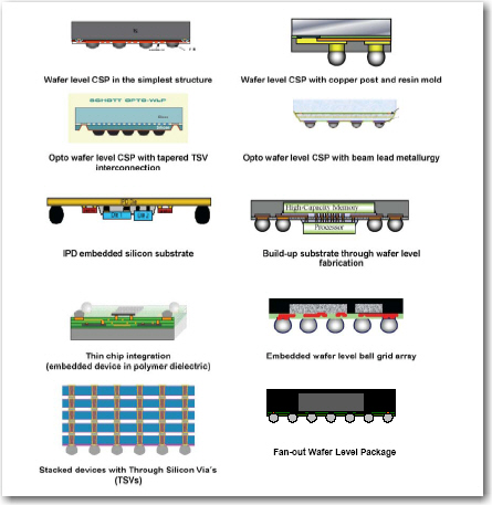
Wafer Level Packaging
Wafer level packaging (WLP)is being defined as a technology in which all of the IC packaging process steps are performed at the wafer level. The original WLP definition required that all package I/O terminals be continuously located within the chip outline (fan-in design) producing a chip size package. From a systems perspective, under this definition, the limitation on WLP was how many I/O could be placed under the chip and still have a board design that can be routed.
However, new packages have recently been introduced which are “Fan-out” WLP. They are processed by placing individual sawn die into a polymer matrix that has the same form factor as the original silicon wafer. These “Reconstituted” wafers are then processed through all of the same processes that are used for “real” silicon wafers, and sawn into separate packages. The die are spaced in the polymer matrix such that there is a perimeter of polymer surrounding each placed die. This area can be used during redistribution (RDL) to “fan out” the RDL to an area larger than the original die. This allows a standard WLP solder ball pitch to be used for die that are too small in area to allow this I/O pattern without ‘growing” the die to a larger size.
Thus WLP technology can now include traditional wafer level chip size packages (WLCSP), Fan-out wafer level packages, wafer level packages with TSV, wafer level packages with Integrated Passive Devices (IPD)s. This is shown in the figure below.
SiP
The roadmap now defines SiP as “…a combination of multiple active electronic components of different functionality, assembled in a single unit, which provides multiple functions associated with a system or sub-system. A SiP may optionally contain passives, MEMS, optical components, and other packages and devices”. These may be arranged horizontally, vertically or be embedded as shown below.

Not much here that we haven’t already covered extensively in PFTLE and IFTLE. Below is a nice graphic from Intel showing the evolution of memory on logic (without timelines). 
There is extensive discussion on chip package co design which the roadmap concludes will be necessary to reduce time to market and cost. There are also discussions on the specific requirements for opto, Rf, MEMS, automotive and LED packaging – the latter certainly being a hot topic recently. [ see PFTLE 123 “LCDs Coming to a Lighting Application Near You”, 3/18/2010 ]
One complaint I have about this document (same as the interconnect document) is that there are far to few primary references contained in the document ( 20 total) Roadmaps like this should be well documented with primary sources.
For all the latest on 3D IC and advanced packaging stay linked to IFTLE…….
……. previous PFTLE blogs are located at www.pftle.net……..
