
The true 3D aficionado has been waiting for the first true commercial product announcement. We already have face to face stacking without TSV (chip-on-chip in the Sony Playstation and many other products) and TSV being used for 1 layer image sensors (nearly all of todays CMOS image sensor manufacturers) but when will we see a true 3D design which will contain (a) TSV, (b) stacking and (c) thinning ?
We were teased this past week with headlines such as “Xilinx Stacked Silicon Interconnect Extends FPGA Technology to Deliver ‘More than Moore’ Density, Bandwidth and Power Efficiency”. I must acknowledge that it does not directly say anything about 3D, but there certainly was a lot of buzz in the industry since the packages make use of TSV interposers.
We have seen a lot of structures recently that use the silicon interposer to mate die to the top and bottom of the interposer (i.e the Renesas SMAFTI) . Last week Xilinx announced a single layer, multi chip silicon interposer for its 28nm 7 series FPGAs. These FPGAs reportedly extend the range of applications programmable logic can address by offering up to 2 million logic cells for high levels of computational performance and high bandwidth.
The 28nm Virtex-7 LX2000Tmulti die FPGA will provide more than 3.5X the logic for capacity of the largest current-generation Xilinx 40nm FPGA with serial transceivers and 2.8X the logic capacity of the largest competing 28nm FPGA with serial transceivers.
Within the Xilinx stacked silicon interconnect structure, data flows between a set of adjacent FPGA die across more than 10,000 routing connections. Compared with having to use standard I/O connections to integrate two FPGAs together on a circuit board, stacked silicon interconnect technology provides over 100X the die-to-die connectivity bandwidth per watt, at one-fifth the latency, without consuming any high-speed serial or parallel I/O resources. By having die sit adjacent to each other and interfaced to the ball-grid-array, Xilinx can avoid any thermal and/or design issues that would be introduced had a pure 3D IC vertical die-stacking approach been taken. This will reduce power, and improve performance compared to a multi-FPGA approach
Xilinx reports that they have been working with TSMC and their assembly house Amkor. The device is made possible by Amkors micro-bump assembly, FPGA architectural innovations from Xilinx, and advanced technology from TSMC. The new products deliver lower levels of power consumption, system cost and circuit board complexity compared to using multiple FPGAs, each in their own package, for the same application.
By using TSV silicon interposer to implement their stacked silicon interconnect approach, Xilinx reported that they “ reduced the risk involved with thermal and design issues of full 3D IC stacking” This probably means that full 3D just is not ready yet and we will be seeing more ”Xilinx like” designs in the near future before we see full 3D in a few years from now.

For more technical information including white papers, visit the Xilinx web page at: http://www.xilinx.com/stackedsilicon.
Amkor /TI Copper Pillar Technology
The week before Semicon West Amkor and TI announced that they had qualified and begun production of the industry’s first fine pitch copper pillar flip chip packages – shrinking bump pitch up to 300 percent compared to current solder bump flip chip technology [link]
Very little follow up was available because of the exclusivity TI was given as part of the joint development program. The publically available data left me once again asking “Where’s the Beef” [ see IFTLE 3 "â??¦on finding the beef and finally addressing 3D IC"]
I was personally told that full technical details are being withheld till the next ECTC conference [ June 2011].
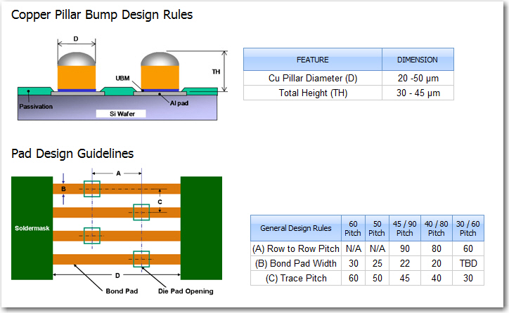
Last week Amkor did release come details on their technology. For all the available information on this technology see the amkor website here (AMKOR) .Design rules are shown below.

Intel has agreed to manufacture a specialized microprocessor design for Achronix Semiconductor at its most advanced factory [link]. While the production use less than 1% of Intels production capacity, it certainly is a departure from their normal business model and may point to their experimenting in the foundry business to keep such options open for the future. While Intel is brushing this off as non important, I would kep an eye out for similar developments.
For all the latest in 3D IC and advanced packaging stay linked to Insights From the Leading Edgeâ??¦.


