ASE – Cu WB
We have previously discussed the significant inroads being made by Cu WB (wire bonding) [ see PFTLE 86 “Advanced Packaging from Rimini”, 07/12/2009 ]. At the ESTC ASE’s Bernd Appelt gave a update on the status of Cu WB in ASE.
Cu WB has been around for some 20 years but up till now has been limited to high power applications with wire diameters over 2 mil. Now that commodity gold prices have surpassed $1000 / oz there is significant demand to drive down the cost of gold WB. Fine diameter Cu wire refers to wire diameters below 1.2 mils, normally 0.8 mil, either Cu wire or Pd coated Cu wire (Nippon Steel).
Gold is very resistant to oxidation and corrosion. . While copper has electrical, thermal and mechanical advantages it also presents challenges due to the mechanical properties as well as its propensity for oxidation and corrosion. To overcome Cu oxidation during electronic flame off (EFO) that leads to a free air ball (FAB) of an undesired appearance, forming gas ( 95% N2, 5% H2) is widely used. Spherical ball shape is a good indicator that an ‘oxide free’ ball has been formed.
According to KNS, the cost of Pd-coated wire is currently about twice that of bare copper wire, but still offers savings over gold wire. The palladium coating greatly reduces oxidation on the surface of the wire. allowing a nitrogen gas atmosphere (no H2) during ball formation. The oxide-free surface of Pd-coated wire also results in a more robust stitch bond with higher stitch bond pull strengths and the shelf life of the Pd-coated wire is longer than bare copper wire.
Al splash, which can be quite pronounced, must be contained within the bond pad opening (BPO) as shown in the Fig. below. Residual Al thickness should be 100 nm minimum. This thickness typically survives JEDEC temp cycling of more than 1000 hrs.

The mold process and pre-mold plasmas do not require any change other than the usual optimizations of plasma. Concerns have been raised about the reliability of standard mold compounds as do to the propensity of oxidation and corrosion of Cu.
ASE reports that reliability has been demonstrated to exceed 2x standard JEDEC testing and is continuing. More than 400 million devices have been shipped by ASE from six different factories. More than 1,500 wire bonders are running with Cu wire and they expected that by the end of 2010 this number will increase to 3,000.
KNS – Thin Die Pick and Place
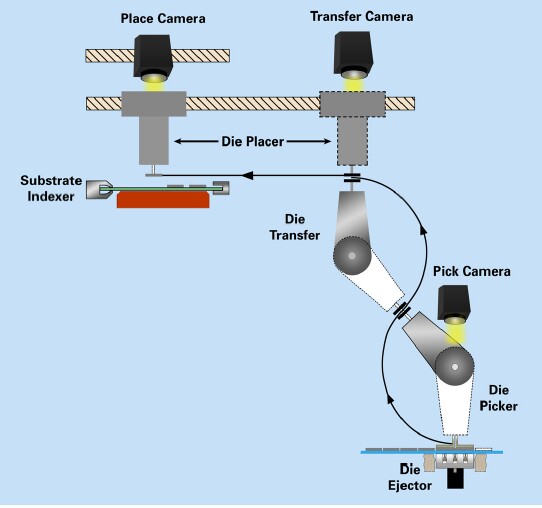
Common attributes to all thin die processes include: 1) relatively long pick times (typically 300 to 600 msec) to avoid cracking of the dice and 2) relatively long place times (500 msec up to 2 sec) in order to guarantee good die attach quality. Peeling the die from the wafer mounting tape typically requires a large vacuum suction force which can be achieved by a large number of large diameter vacuum holes. On the place tool, however, the large vacuum holes need to be avoided in order to minimize the die deformation during the place process, since this can lead to undesired air inclusions (voids) between the die and the substrate or the underlying device. KNS describes their parallel pick and place architecture (shown below) which they claim both units per hour and die attach quality. With the parallel pick and place architecture the pick process of the subsequent die can already be initiated during the place process of the first die.
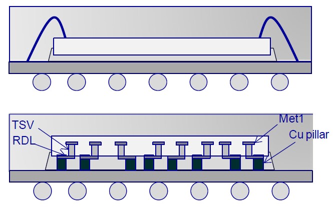
ST Micro, ST-Ericsson and CEA Leti showed results of their study comparing a wireless video product built and compared in WB vs TSV constructions.
Chips were fabricated using a 65nm node CMOS process including seven Cu metal layers with low-k. TSV were 60μm diameters on 120μm pitch in 120μm thick wafers. Cu pillars used for die to substrate connection were 70μm diameter on 130μm pitch and 80μm height. The BGA package (4x4mm) included 65 balls on 0.4mm pitch.
On Semi – Low Profile WLP
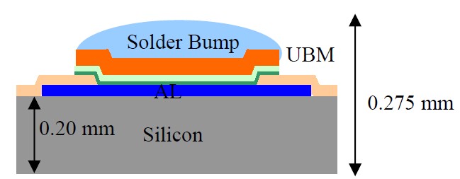
To meet requirements for thin smart phone products, ON Semiconductor has developed “LPCSP” a low profile CSP (WLP) with a 0.275 mm thickness.
IMEC / Amkor – Reliabilty of Cu-Sn IMC Microbumps in 3D Stacking
IMEC and Amkor have studied thermal cycling and electromigration, on fully packaged Si-to-Si stacks bonded with Cu-Sn intermetallic (IMC) micro-bumps.
While the presence of small voids at the interface between Cu and Cu3Sn becomes more pronounced with continued ageing, during thermal cycling, these voids do not affect the daisy chain resistance during temp cycling between -40 and +125 C. The Cu-Sn IMC bumps survive thermal cycling for more than 3900 cycles.
Resistance to electromigration appears strongly dependent on Sn thickness showing an improved performance for thinner (3.5 µm) vs thicker (8 µm) Sn. For 8 μm Sn bumps, almost all available Cu is fully consumed (5μm on each side of the joint) and the Cu3Sn phase reaches the Cu damascene layers. Voiding inside these thin layers is reportedly detrimental to the interconnection stability. A more conservative ratio of Cu and Sn is therefore suggested.
While IMC bumps outperform standard solder flip chip bumps, the authors recommend that an overall reduction of the void formation may be advisable for further reliability improvement.
They conclude that appropriate packaging of these Cu-Sn IMC bonded Si-stacks results in overall excellent thermo-mechanical and thermal-electrical behavior for various reliability test conditions which makes them highly suitable for connecting fine pitch advanced substrates.
Amkor – Wafer Level Fan Out
When it comes to fan out WLP Amkor has appeared behind Infineon partners STATSChipPAC and ASE. Amkor presented wafer level fan out technology developments using Ajinomoto build-up film (ABF), laser ablation via generation processes and buried pattern PCBs, which they claim results in low cost and high electrical performance.
In the first process ABF is laminated to the reconstructed compression molded wafer, micro-vias are formed by laser drilling and Cu RDL interconnect is plated and pattern defined.

Fraunhoffer IZM – Thin Stackable Embedded Chip Packages
In two separate presentations researchers from Fraunhoffer IZM and coauthors detailed now methods to construct thin stackable packages.
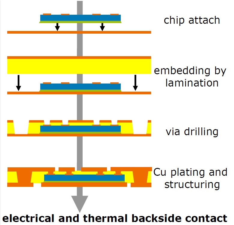
Under the framework of the EU-funded project “HIDING DIES” program industry and research organizations worked with Fraunhofer IZM to develop embedding technology based on embedding thin chips into build-up PCB materials. Electrical contacts to the chips are realized by laser-drilled and metalized microvias. A follow up EU-funded project “HERMES” has the broader scope of furthering the embedding technology and bringing embedding technology into production with the goal of embedding components in 18 x 24 inch PCBs.
Dies can be either placed face-down on the substrates or face-up. The Fraunhofer IZM technology focuses on the face up approach in combination with the formation of laser micro vias. The process flow is shown below using resin coated copper (RCC) to embed the die:

A QFN package results when the chip is attached to a metal substrate as shown below. Both top and bottom contacts are directly accessible for better heat dissipation which is of importance for devices like power chips.
Infineon – eWLB
Infineon presented the latest developments in connection strategies for 3D-eWLB and the challenges of the technology this development.
Multichip- eWLB – a minimum distance between two dies is set, depending on amongst other things the size of the filler particles. Typically the minimal fillable gap is 2.5 times the maximum filler size, but this is also depending on the thickness of the silicon die(s). They report excellent mold compound filling behavior of 250 μm die to die gap. After the pick and place process step, no special multi-die specific process step are reportedly needed. The wafer is molded with standard mold compound and the same dielectrics and redistribution lines are applied as for the single die eWLB. Die shift and wafer warpage after molding was found to be equal to single die eWLB. Reliability testing including Temp cycling and BLR drop testing showed no difference between eWLB and multichip eWLB.
Stacked eWLB (or ePoP) – the technical advantages of eWLB PoP stacking are reported to be :
– Low profile and small lateral dimensions
– No interposer requirement (reduced number of interconnects, reduced cost)
– Use of top packages with standardized ball array
Connection in z-direction for a “ePoP” package can reportedly be realized in two ways.
– drill via holes by laser
– via bars, produced in PCB technology, can be molded into the reconstituted wafer
The process flow for the latter is shown below. The chips and the PCB based bars are placed on the mold carrier and the reconstituted wafer is generated via compression molding. After reconstitution the artificial wafer is ground down to make the via bar accessible for the connection with a redistribution layer. It consists of a dielectric on bottom side, redistribution layer and solder stop on top and bottom side. 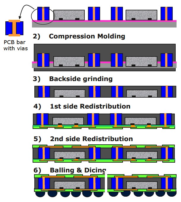
Hope to see many of you at next weeks RTI 3D-ASIP conference in Burlingame CA (link)
For all the latest on 3D IC Integration and Advanced Packaging stay linked to Insights From the Leading Edge, IFTLEâ??¦â??¦â??¦â??¦â??¦â??¦â??¦
