Penn State
Yuan Xie from Penn State and IBM collaborators from the System and Technology Group took a look at 3D IC thermally-aware bus optimization.
Given that :
– TSVs are clustered for both signal and power delivery
– TSVs are duplicated (redundancy as high as 20x) for higher reliability and higher yield
What is the impact of these TSV clusters on 3D thermal profile ?


The Tech Design Forum ( formerly EDA Tech Forum), has been restructured to focus on fast-growing technology markets in specific regions and has added panel discussions of industry and media experts, as well as technical sessions. They will hold the following meetings in 2011:
March 10 – Santa Clara; April 11 – Tel Avivl; July 20 – New Delhi; July 22 – Bangalore; August 25 – Tokyo; August 31 – Shanghai; September 6 – Beijing; September 8 – Hsin-Chu; September 8 – Santa Clara.
The March 10th Tech Design Forum "EDA Edition" focused on IC Design and Verification, exploring ecosystem networking and increasing competiveness in IC and system product development. The keynote by Dr. Mario Paniccia, Intel Fellow, titled "Bridging Photonics and Computing" discussed recent advances in silicon photonics, including the first silicon photonics optical link operating at 50 Gbps, the scalability of this technology and its potential applications.
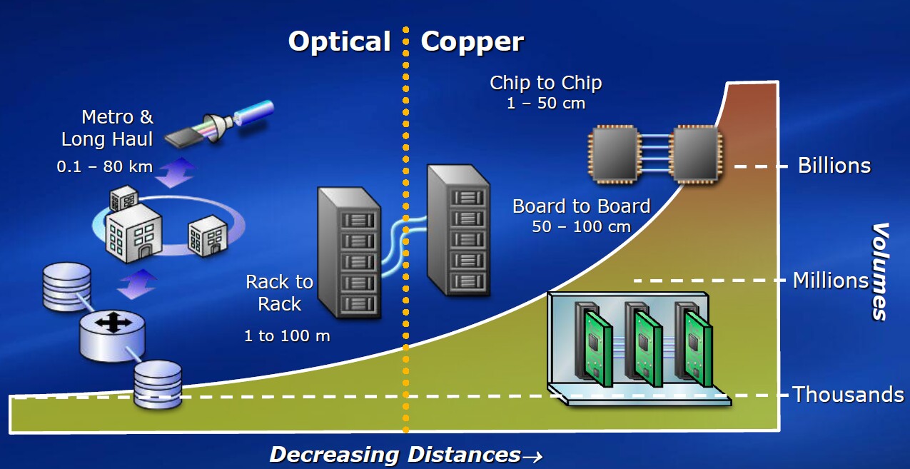
Intel asks the question ��?With all the data that is moving and will need to be moved, how do we connect all these devices?


We have previously discussed what appears to be the planned move of Applied Materials into the IC packaging space [ see PFTLE 72, ��?Samsung 3-D ��?Roadmap��? That Isn��?t��?; PFTLE 41, ��?3D Integration Stays HOT at Semicon West��? ]
Applied Materials has now signed an agreement with Singapore��?s Institute of Microelectronics (IME) to set up a Center of Excellence in Advanced Packaging in Singapore. The Center, to be located at Singapore��?s Science Park II, will focus on new capabilities in advanced packaging. When finished, this advanced semiconductor packaging RandD facility will enable IME to support Applied Materials��? product development initiatives. The Centre will have a full 300 mm line of Wafer Level Packaging (WLP) and 3DIC processing equipment and will conduct research in semiconductor hardware, process, and device structures.
Applied expects many advanced logic devices at the 40nm and below technology nodes to be packaged at the wafer level. Russell Tham, Regional President – South East Asia, said, âÂ??Â??This collaboration is to âÂ??¦. (bring) our development activities closer to our customers in Asia.âÂ??Â??
For all the latest in 3D IC and advanced packaging stay linked to IFTLE……

