Several of you at Semicon West requested that I make the figures larger (i.e more readable). I am stuck with the limitations of "blogger" software which is very HTML sensitive but I will try.
Anyway, this week we will continue to take a look at packaging activities at the 2011 ECTC.
IMC formation in fine pitch microbumps
Samsung found that Ni3Sn4 IMC formations at interface between SnAg solder and their 4µm Ni UBM degrades the mechanical properties of solder joint, and increases resistance of solder bump. IMC growth rate and Ni UBM dissolution rate were calculated.

Thin IMC changes into thick IMC during HTS. During 150°C annealing for 1300 hours, Ni UBM was converted into Ni3Sn4 IMC. Even though there are such microstructure changes, resistance of micro bumps were not changed during HTS 150°C. Resistance started to degrade after 1000 hours at 180°C due to void formation at interface between IMC and Al trace line. They found that open failure occurred when Ni UBM completely consumed and failure time is consistent with total consumption time of Ni UBM.

ITRI reported similar results on their 12µm microbumps (5µm Cu/3µm Ni/2.5µm SnAg) on 20µm pitch. The intermetallic phase formed at the interface was identified as Ni3Sn4, the thickness of this layer increases with time and/or temperature in agreement with the results of Samsung. They also found problems with seed undercut during processing. When the thicknesses of the Cu seed layer sputtered on the wafer was reduced from 5000Å to 2000Å and a dry etching was used to remove the seed layer after bump plating and PR stripping, the undercut of Cu posts could be confined to less than 10%. A dramatically undercut Cu pillar (left) takes on the appearance of mushroom plating.
ITRI reports that conventional reflow with flux is seldom used for the assembly of microbumps because the gap size between chip and interposer, i.e. 20µm, makes it difficult to remove flux residues which could cause void formation within the underfill and degrade the reliability.
Copper pillar bump on lead
Qualcomm and STATS ChipPAC reported on the unique combination of copper pillar bump and bump on lead (more accurately called bump on trace). Their suggested acronym CuBOL just doesn’t identify the structure well enough for me, so I prefer and humbly suggest CPBOL for copper pillar bump on lead.
The technology which utilizes the fcCuBE technology of STATS ChipPAC (see USP 7368817), involves using Cu pillar bump attached to a narrow trace or "bond-on-lead (BOL)" without any solder resist confinement (open SR) in the peripheral I/O region of the die. This enables improved routing efficiency on the substrate top layer thus allowing 4L to 2L reduction in the substrate without compromising functionality. The cost of the FC package is lowered by means of reduced substrate layer count, removal of solder on pad (SOP) and solder mask and relaxed design rules. BOL or narrow pad which takes significantly lower space on the top layer allowing more area for escape routing; thus enables relaxed Line / Space (L/S) design rules which in turn help to lower the substrate cost significantly. Similarly, the ‘Open SR’ concept in CuBOL further allows additional escape routing to be fit in the same bump-to-bump spacing; which offers increased routing efficiency and I/O density on the top most layer. The combination of BOL and Open SR together thus allows conversion of 4L substrate design into 2L without compromising I/O density.

Fluxless chip-on-wafer (C2W) bonding
ITRI reported on their studies fluxless joining of 30µm pitch Cu/Ni/Sn-Ag bumps. In this study, the Ar + H2 plasma treatment was applied on the C2W process for the purpose of tin oxide removing and enhancement of the bondability. During bonding they found that gap control was very important since poor control could lead to a narrow necked joint ( c) or solder ozzing out of the joint and possible causing shorts (b).

After bonding and underfilling, temperature cycling test (TCT), high temperature storage (HTS) at 150°C, highly accelerated stress test (HAST) and electromigration (EM) reliability were performed on the chip stacking module to evaluate the reliability of solder micro bump interconnection assembled by the C2W process. Without underfilling a significant number of samples failed . With underfilling HTS greater than than 2000 hrs; TCT greater than 3000 cycles and HAST testing were confirmed.
Reliability of Xilinx interposers
Xilinx shared some of the reliability data on their 28nm FPGA with interposer structured. Recall the chips and the interposer are manufactured by TSMC, the interposer is bumped by TSMC, and the chips are bumped by Amkor. The final assembly is done by Amkor [see IFTLE 23, "Xilinx 28nm multidie FPGA…"]
The silicon interposer test chip with thousands of micro-bumps at 45µm pitch has been fabricated.
The silicon interposer is 100µm thick, and is mounted on a 42.5mmÃ??42.5mm substrate through 180µm pitch C4 bumps. The TSVs are typically 10-20µm in diameter and 50-100µm deep. The walls of the TSV are lined with SiO2 dielectric. Then, a diffusion barrier and a copper seed layer are formed. The via hole is filled with copper through electrochemical deposition. The interposer wafer is thinned to expose the TSV from the bottom side. The Cu overburden is removed by CMP followed by passivation and UBM process. C4 bump is electroplated and reflow soldered on top of the UBM layer. FPGA wafers are bumped to ultra-fine pitch in the range of 30-60µm using Cu pillar bump technology. The FPGA dies are diced and attached to the interposer top pads. The gap between the interposer and the FPGA die is filled using underfill material to protect the micro-joints. X sections of the overall assembly, the interposer and the micro joints are shown below.
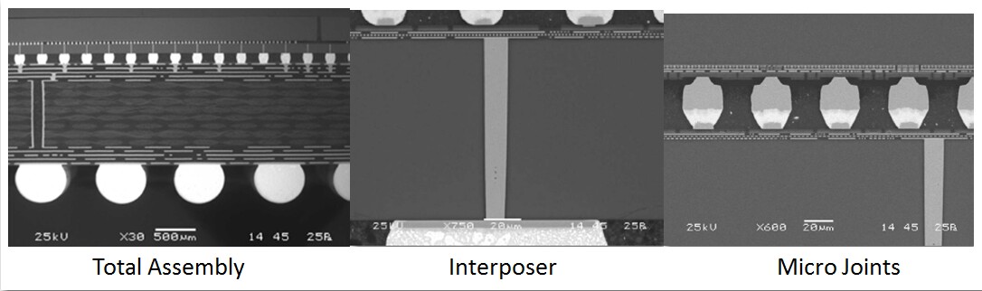
Main focus of this study was to understand the impact of moisture and temperature cycling on the microbumps and adhesion of the underfill to top FPGA die and thin TSV interposer substrate. Underfillls were first evaluated and found to perform better with no clean flux. Plasma cleaning was implemented before underfilling and gap height was increased to improve underfill flow.
With improved gap height and plasma cleaning, no delamination was observed either in L5 preconditioning or after 264 hrs of HAST at 110°C. All the samples passed 1000 cycles of TCB. Cross-sectioning of interposer after 1000 cycles confirmed that there was no protrusion of TSV. An example of cross-section of micro joint after 1000 TCB cycles.
Fraunhoffer through mold vias
Fraunhofer IZM examined chip embedding into polymer by molding and redistribution by PWB technologies for highly integrated low cost packages.

The general process flow starts with the lamination of an adhesive film to a carrier. This adhesive film has one pressure adhesive side and one thermo-release side (heating the tape, the thermo-release side of the tape loses its adhesion strength). Dies are placed, active side down, towards the carrier. Molding is done by large area compression molding. For chip redistribution, resin coated copper is used. After lamination of the RCC film on both wafer sides in one step, micro vias are laser drilled to the die pads and through mold vias in the same process step to connect to and bottom side. By plating both, via filling and die pad connection to the copper layer and the top copper layer to the bottom copper layer are achieved.
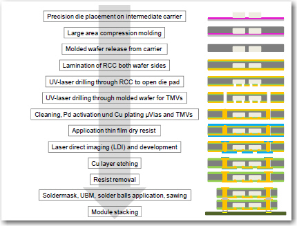
Mold materials with small filler particles (maximum filler particle size of 25µm) allow the fabrication of vias with a very precise and smooth via surface but materials with finer fillers currently have higher viscosities and lower filler content leading to a higher CTE.
For all the latest in 3D IC and Advanced Packaging, stay linked to IFTLE…
