Polymer filling technology for Vias last (backside) TSV


Leti presented informative data on polymer filing of vias last (backside) TSV. The normal Leti process a wafer is bonded on a temporary glass carrier and thinned down to 120µm. 40-60µm diameter vias are then performed by DRIE in silicon. A 2µm thick SiON insulation layer is performed by PECVD. A plasma etching is then performed to open contacts on metal level in TSV bottom. Due to the TSV dimensions complete filling with a metal is not appropriate due to issues including process time, process cost, metal overburden thickness and thermo-mechanical stress. For these reasons, a copper liner is electroplated inside the TSV. This liner also forms the RDL layer on the wafer bottom surface. A 7µm thick polymer layer is then coated on the RDL in order to insulate it This layer, realized by spin-on of a liquid polymer, tents the RDL and TSV without filling it, as shown in the figure below. This leaves the copper liner inside the TSV exposed to trapped air (oxidation). In addition, the thin polymer layer over the TSV is a weak point where temperature variation (during following process steps or device lifetime), can break or crack the layer.

In the modified "polymer fill" process a 20 to 30µm thick polymer layer is coated by spin-on on the wafer. Vacuum heating is performed decreasing the polymer viscosity and allowing easier removal of the air trapped in the TSV. Temperature and the pressure during the vacuum heating has to be optimized for each different polymer in order to obtain complete filling of the TSV.
Trials have been done with two polymers having different thermomechanical properties (see table ).
Polymer 1 has a higher Young modulus and a lower coefficient of thermal expansion than polymer 2. Results show that polymer 1 induces more warpage in the thinned wafer than polymer 2

Fan Out WLP by RDL first Method
Researchers at Renesas described a unique process flow for achieving fan out WLP (FOWLP) by an RDL first method. The fabrication technology used for most FOWLPs is a chips first method (shown in the figure below) where the chips are mounted to a carrier face down; the chips are molded into a wafer and the carrier removed; RDL and terminations are formed and the packaged chips subsequently singulated. Renesas repots limitations to this process flow include (1) The I/O pitch of the embedded chip is limited by alignment mismatching between the chip and the RDL; and (2) The RDL requires a low-cure temperature resin which may negatively affect package reliability.
Renesas suggests a RDL first approach which they note is based on their earlier work with NEC on the SMAFTI program ( smart chip connection with feed through interposer). The process flows are compared below.
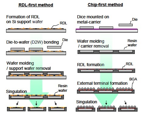
They claim that a finer chip I/O pad-pitch is achieved due to better CTE matching between the die and support wafer and that the high-cure-temperature resins used, make the RDLs more reliable. Their name for this is SiWLP for SiP (system in package) WLP. Another acronym I greatly dislike since it will always be interpreted as "silicon WLP" for obvious reasons.
The figure below compares a WB-BGA solution to a SiWLP solution for a 6 mm2 analog chip and a 3 mm2 microcontroller. It indicates that the SiWLP enables a 57 % reduction in area compared to conventional WB-BGA-type SiP.

Mechanical Properties of Thin Film Polymers
A joint publication between RTI Int, U Texas-Austin and Microelectronic Consultants of NC took a close look at the mechanical properties of low temp ( ca 200 C) cure polymers [Asahi Glass-ALX; Hitachi-DuPont-PBO and JSR-WPR 5200]used in RDL type applications. Getting thin film specimens [10-20µm thick samples] properly fabricated and loaded into a test system is not a trivial task. Reproducible data requires samples that are lithiographically prepared (not cut with a razor blade) and requires compliance correction factors be calculated. The following table shows vendors reported data vs data gathered in this study. Manufacturer reported modulus numbers were in all cases off significantly (ca 50%) and in some cases elongation and tensile strength numbers showed quite a large spread indicating that even in this study, where extreme caution was taken to prepare the samples, flaws must have been present.

Tezzaron
PFTLE and IFTLE have previously covered Tezzaron, one of the pioneers in 3D IC [ see PFTLE 125, PFTLE 115, PFTLE 90; IFTLE 8, IFTLE 28]
We recently revealed that MOSIS working with Tezzaron and Mentor Graphics would now allow users to test out 3D-IC concepts using the standard Tezzaron 3D process. [link]
MOSIS is gathering participants and will manage the program. Tezzaron CTO Bob Patti reports that they will "…provide the PDK (design kit), assist with 3D design issues, do the 3D assembly, and deliver the finished components".
Patti also reports that their 3D IC customer program activity is increasing exponentially. Since customers have not identified themselves publicly, Tezzaron cannot say who they are. They also aren’t at liberty to describe the chips in any detail, however Patti indicates that the devices include:
– More than one multi-core processor – Smart temperature sensor
– Synthetic aperture radar processor – ADC based I/O receiver
– Cellular automata FPGA system – Synchronization and power delivery architectures

For all the latest on 3D IC and advanced packaging stay linked to IFTLE…..
