This week, lets take a look at some of the presentations from the Suss MicroTech workshop “3D Integration – Are We There Yet” which was held at Semicon West in July.


Eric Beyne, IMEC Scientific Director for 3D Technologies, addressed the technical issues of carrier systems for 3D TSV thinning and backside processing. Beyne points out that right now silicon carriers are favored over glass because the glass, while transparent which allows for laser based optical debonding techniques, must be CTE matched to silicon over a large temperature range; ground to tight TTV specification (high cost ?) and has a negative effect on plasma based post grinding backside processes due to its low thermal conductivity.
After alignment and temporary bonding Beyne recommends the use of use of in-line metrology to allow for wafer rework if necessary.

Rama Puligadda, Mgr. for Adv. Materials R&D for Brewer Science gave an update on their ZonebondTM room temperature debonding process. The Zonebond process basically uses a 2.5 mm ring of adhesive to hold the wafer in place for grinding and backside processing which allows for easier subsequent debonding. The thin wafers are released from the carrier at room temperature after mounting on a film frame. Blanket UV exposure on the flex frame allows solvent removal of the temporary adhesive without damaging the adhesion to the flex frame tape.

Brewer has also developed a process with two carriers in order to achieve a wafer flip.


Stephen Pateras, Product Marketing Dir. at Mentor Graphics, gave a presentation on advanced design for test (DFT) and built in self test (BIST) for 3D-IC structures. Pateras points out that TSVs can be used to create test access paths so that all BIST resources can be accessed on any device.
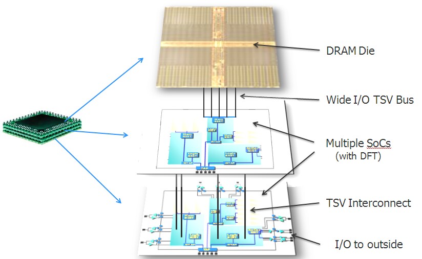
Pateras also concluded that all EDA players need to support common test access infrastructures since this will be required to stack die from difference sources.
Eric Strid, CTO of Csacade Microtech, indicated that they are using MEMS techniques to produce lithographically printed probe cards capable of 6 µm sq. x 20 µm high probe tips on 40 µm pitch which are being sold in research quantities.

Strid pointed out that standard pad locations will be required for vendor interchangeability and that standard materials specs for pads are needed in terms of materials, thickness and flatness. Such standard pad locations will enable standard test tooling.
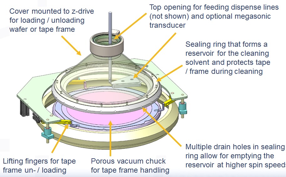
Stefan Lutter , Bonder Project Mgr for Suss, discussed equipment and processes for temporary de-bonding. Suss reports that their open platform approach is capable of using any of the following bond/debond technologies. They see the industry trend as moving to the newer room temperature (RT) release processes.


They claim that their HVM equipment, available 4Q 2011, will be capable of bonding and debonding 20-25 wafers/hr. The new Suss MicroTec product introduction is a HVM debonder/cleaner line for the RT release processes.

Thinned wafer on carrier mounted to flex frame are fed to these modules and thinned wafer on flex frame and detached carrier are generated. The technology uses a porous vacuum chuck to hold the thin device wafer that is mounted on tape and a flexible plate with vacuum grooves and debond initiator to peel-off the carrier. A schematic of the cleaning process is shown below.
For all the latest on 3D IC and advanced packaging stay linked to IFTLE


