In Feb 2005 my first article on the topic âÂ??Â??Future ICâÂ??Â??s Going VerticalâÂ??Â?? was published in Semiconductor International predicting that the industry would eventually have to move in this direction. A short month later, March 2005 I felt like a prophet when a TSV based 3D stacking approach was described by IntelâÂ??Â??s Justin Rattner (todays CTO) at the Spring Developer Forum, with statements like âÂ??Â??…stacked wafers and stacked dies using thru-silicon vias are showing promise in meeting the memory bandwidth challenge.âÂ??Â??
A year later, in April 2006 headlines from Soeul read âÂ??Â??… Samsung has developed a new "3D" package, which reduces space requirements and increases performance capabilities of today’s multi-chip packages. The company plans to use the technology to improve its NAND Flash packaging starting in 2007âÂ??Â?? Samsung announced that its new wafer-level processed stack package (WSP) rather than using wire-bonding …. micron-sized holes that penetrate through the silicon vertically to connect circuits directly – TSV. According to Samsung the technology would enable manufacturers of mobile and consumer electronics devices to achieve better electrical performance and design slimmer and high-performance handset designs that provide improved battery time. The announced that the technology would enter mass production in 2007, for NAND Flash packages initially. And that they planned to use WSP for server DRAM stack packages sometime down the road.
Now, thirteen years later ASET is in its 3rd incarnation ��?the Dream Chip program��? , it is obvious that DRAM will be stacked before NAND flash hopefully in HVM by 2013 (not 2007) , IBM has announced a major memory program with Micron (though not in 2008) and we are still awaiting any word of commercialization from Intel. Certainly it��?s fair to say that this is taking a bit longer than we all thought, even those of us who were trying to be ultra conservative.
Micron has announced that they will be manufacturing the memory layers and have contracted with IBM to manufacture the logic layer. Micron will be doing the assembly of the layers at a yet to be disclosed location. For now we can assume they are doing the initial production in Boise. For our initial discussions on this technology see IFTLE 74, ��?The Micron Memory Cube consortium��?.
The technology described by M. G. Farooq of IBM last December at the IEEE IEDM [ see IFTLE 82 âÂ??Â??3DIC at the 2011 IEDM…âÂ??Â??] is the technology being used to create the logic layer in the HMC stack (blue layer).
(Click on any of the pictures to enlarge them)


Chipworks has concluded that â�?�? it appears that the TSVs are annular. Once the lower metal / dielectric stack is formed (including the via dielectric for the metal layer that contacts the TSVs), the TSVs are drilled through to the silicon, and then a Bosch etch is used to drill the vias about 100 µm into the substrate, with a minimum pitch of 50 µm. After drilling, a conformal oxide is deposited, the barrier and seed layers are sputtered in, the copper fill is plated in, and any excess copper is CMPâ�?�?d off. The dielectric for the contact level metal is put down, and then the top fat-wire metal levels are conventionally defined.â�?�? [link]
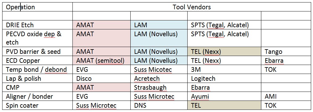
TEL acquires Nexx
Tokyo Electron Limited (TEL) has acquired semiconductor packaging equipment supplier NEXX. Nexx advanced deposition equipment, including electrochemical deposition (ECD) and physical vapor deposition (PVD) tools will be added to the TEL line of products aimed at back end packaging applications and 3DIC.
Long time readers know that this has been a theme identified by IFTLE [ see PFTLE 41, ��? 3D Integration Stays Hot at Semicon West��? or PFTLE 107 "3D News:Applied/Semitool, TSMC, Ziptronix��?
Looks a lot like the front end heavy weights Applied, LAM and TEL are going to buy up all the pieces they need to become the 3 heavyweights in packaging and 3D. Consolidation will continue because with fewer and fewer players moving to 22 nm and beyond packaging is a natural evolution for some of these big front end equipment vendors.