Design Automation Conference 2012
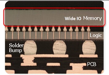
At the design automation conference in June Samsung, who has been on absolute lockdown when it comes to 3DIC materials leaking out of the company, opened the door…just a little bit with Samsung foundry indicating that they will be ready to release 3D TSV Technology and Wide IO Memory Solutions "in early 2013."
Samsung’s message as to the major attributes of 3DIC vs a package on package solution (PoP) are summarized in the slide below:
(Click on any of the images below to enlarge them.)

In terms of wide IO memory solutions they report that they will have wide IO DRAM (Non-JEDEC type ball interface) ready for customer sample in early 2013 and will also have JEDEC standard wide IO DRAM2 .
They claim that TSV PDK and Design Methodology has been proven for 32nm node:

Not a lot of info, but at least an official indication that Samsung foundry is getting ready and we should be seeing products in les than a year.
Larger Silicon Interposers are Coming
Up to now, silicon interposers have been limited in x,y dimension to the field size of the steppers being used or 35 mm sq. It is no coincidence that the size of the Xilinx FPGA interposer is 35 mm.
At the recent Semicon West, USHIO (link) introduced a large-field stepper lithography tool targeting interposer fabrication for 2.5D/3D semiconductor packaging applications.
Using a 70 mm projection lens the new litho tool is capable of a 50 x 50 mm field size. They are also indicating that by 2013 they will be introducing 100 mm projection lens, which will increase the field size to 70 x 70mm. Overlay accuracy is reportedly less than 500nm. Alignment is IR transmission based.
EVG Wafer Bonding System first to Pass Equipment Maturity Assessment at Sematech
EVG announced that its GEMINI Automated Wafer Bonding System has become the first product to pass a systematic, rigorous Equipment Maturity Assessment (EMA) implemented within SEMATECH’s 3D Interconnect program. The Sematech assessments are designed to determine equipment readiness for high-volume manufacturing (HVM).
The EVG GEMINI exceeded Level 3 equipment maturity requirements — the highest assessment rating awarded before transfer of new manufacturing processes into pilot lines or HVM. Temporary adhesive bonding, silicon fusion bonding, and metal thermocompression bonding processes have been investigated on 300-mm wafer bonding system installed at CNSE in Albany, New York.
SEMATECH qualified wafer bonding alignment accuracy of less than 500 nm exceeding the wafer alignment specs of the ITRS for 2018. Sitaram Arkalgud, director of SEMATECH’s 3D Interconnect program indicated that EVG is the first company to pass ISMI’s Equipment Maturity Assessment methodology.
For all the latest in 3DIC and advanced packaging stay linked to IFTLE………………….
