EVG
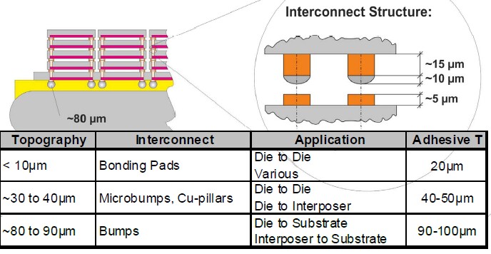
Markus Wimplinger of EVG addressed "Thin die stacking for wide IO memory-on-logic." EVG points out that adhesive thickness for temporary bonding is dependent on the topography being covered, as shown below.
When examining solder reflow bonding and thermo-compression bonding, EVG concludes that reflow soldering does not work for fine pitch bonding (less than 40μm; see Amkor disc above):
– Dies are very thin. Stress causes dies to bend. No mechanical contact between interconnects
– Fine pitch required reduction of solder volume. Reduced solder volume results in lower tolerance for height variations and / or bow and warp of chips
Thermocompression bonding which is becoming standard for fine pitch interconnect has a typical cycle time of 4-16 sec.
SEMI
Dan Tracy, director of industry research and statistics for SEMI, presented their 2012 "Fab equipment and materials market update." Of interest in the TSV materials forecast (obtained from Linx Consulting) is their claim that "bonding adhesives" accounts for >50% of the current (2012) ~$25MM market and still has >45% of the projected 2016 $450MM market. The "cleaning" number of ~22% in 2016 is also remarkable. Since IFTLE has found no temp adhesive materials suppliers willing to quote a current or future price for the materials, we find these numbers, as the Japanese would say, "very difficult."

Cadence
Jiayuan Fang of Cadence presented "Exploring silicon interposers through system co-design and co-analysis to maximize performance." He offered the following interposer system design flow:

Yole
In the market trends forum, Baron of Yole Développment addressed "3DIC and TSV interconnects: 2012 business update." Their latest TSV chip wafer forecast is shown below:

Yole is forecasting that the IBM’s Power 8 chip and the Intel Haswell and the Sony PS4 will all be based on 2.5D interposer technology. [see IFTLE 88: Apple TSV Interposer rumors; Betting the Ranch ; TSV for Sony PS-4; Top Chip Fabricators in Last 25 Years] The Sony GPU + memory device may look something like the Global Foundries demonstrator shown below.

Yole projects the silicon/glass interposer substrate market reaching $1B by around 2016, at which point it will have penetrated ~10% of the IC substrate packaging market.

Both Micron and Samsung have announced that they will be ready to release wide IO 3D stacked memory in 2013.
Corning Glass
In the Executive Summit Forum, Peter Bocko, CTO of Corning Glass, gave a presentation entitled "Glass: Enabling next-generation, higher-performance solutions." While glass has currently been shown to function as a carrier during the thinning operation, the case is made that glass can be used as the interposer substrate. The ability to produce roll-to-roll or on large panels is the driving motivation.
Quoting reports from the GaTech consortium, Corning points to glass interposers showing less warp during chip assembly, faster signal propagation, and significantly reduced signal loss. In fact, they found a 10Ã?? lower signal loss in glass for a 6Ã?? longer interconnect. Such a 60Ã?? lower leakage improves power efficiency.

Significant advancements are being made in fabricating and filling TGV (through-glass vias) as can be seen in the figure below.

For all the latest in 3DIC and advanced packaging stay linked to IFTLE………………………….
