Sitaram Arkalgud outlined SEMATECH’s comprehensive 2.5/3D program which includes:

They see bonding going through an evolution which leads towards thermal compression copper-copper bonding on a less than 30μm pitch. Arkalgud reported that current copper-copper bonding occurs at 400°C with a throughput of 0.5 wafers/hour. The SEMATECH goal is to develop a process that can improve on both of those criteria.

They claim to have demonstrated a low time / temperature process (245°C / 5 min) on patterned wafers and have a tool concept proposed which could increase wafer throughput to 30 WPH.

The current SEMATECH roadmap for copper-copper bonding and thin wafer handing is shown below.

Jon Greenwood of GlobalFoundries shared their thoughts on "collaboration" and how important this is for complex infrastructures like 2.5D or 3D. Since both UMC and GlobalFoundries appear to be behind TSMC in the introduction of a qualified 2.5D process [see IFTLE 122: TSMC officially ready for 2.5D, Apple order impact on TSMC] and they have both publically supported a collaboration approach vs. the TSMC "one-stop shopping approach, presenting arguments for this approach was not unexpected. Greenwood indicated that 3D is being focused in Fab 8 in NY while 2.5D solutions are being focused in Fab 7 in Singapore. Process development was done in conjunction with IMEC in Belgium and Fraunhoffer ASSID in Dresden. They specifically call out the Big 4 OSATS as their assembly partners.

Matt Nowak of Qualcomm, long an advocate 3D technology, reported that Qualcomm has now built "thousands of parts" and does not see anything stopping high-volume manufacturing (HVM) except cost.
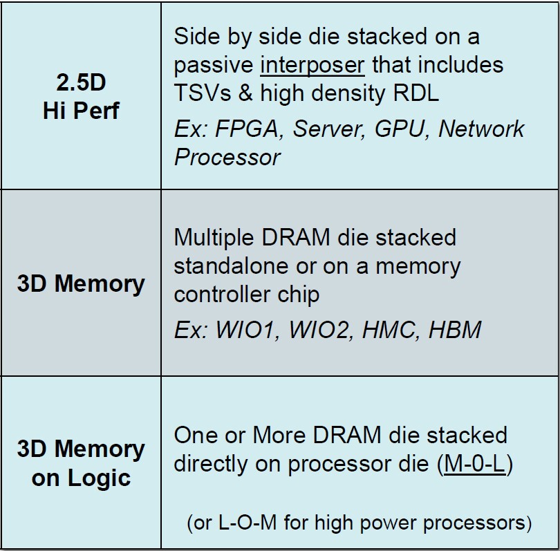
Qualcomm defines high density for 2.5/3D as: 5-10μm TSV, AR ~ 10:1; 1K-10K TSV / μbumps; 10’s μm bump pitch. They see the following categories evolving:
Nowak indicates that Qualcomm will require a price of ~$2 for a 200 mm2 high-density silicon interposer. The high-density aspect is out of the reach of those proposing low-cost "coarse" interposer fabrication and the pricing appears significantly out of reach for the pricing structure for dual damascene foundry-based fine interposers.
For all the latest on 3D IC and advanced packaging, stay linked to IFTLE………………
