Ahmer Syed of Amkor took a look at micro bump electromigration issues. Issues inherent to electromigration have been around a long time [see IFTLE 56, "Electromigration at the 2011 ECTC"]. It is known that current densities on 10K A/cm2 will induce EM within a few hours.

When we look at 2.5/3D we have radically changed the dimensions involved as shown below.

There is a 20�? increase in interconnect density from BGA to μbump and a 10�? reduction in pitch and ball diameter. Yet for the μbumps shown below they saw no failures even after 16K hrs of operation.

They conclude that:
– For WLCSP and BGA joints, they see Cu consumption and failure around the circumference
– For μbumps, they see copper conversion and IMC formation either during assembly or during current/temp stressing, but they see very long life
– While current carrying capacity for BGA and FC joints are in the expected range, μbumps can carry much higher current than theoretically predicted.
– Cu pillar bump interconnects provides the highest current carrying capability.
Nagesh Vordharalli of Altera quoted an IMEC study which shows that the sweet spot for maximum bandwidth will come from interposers with RDL lines/spaces ~3μm. Nagesh feels that silicon based interposers need to be in the 1-2 cents/ mm range to compete with future high density laminate technology.
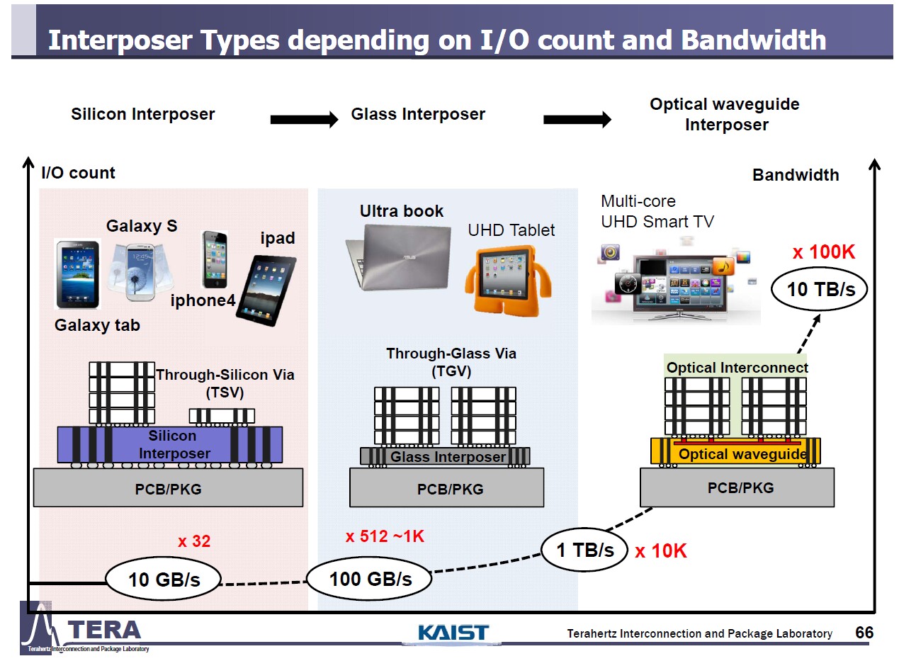
Professor Joungho Kim of KAIST shared his assessment of Si vs. glass interposer electrical performance. Imajo developed comparative data for double sided interposers with 10μm TGV/TSV on 40μm and 100μm pitch. TSV had oxide insulator thickness of 0.5μm. He proposes that interposer type will depend on IO count and bandwidth requirements as shown below.
Nobu Imajo of AGC reported on their ongoing activities to develop low-cost, high-density glass interposers. AGC is looking at EN-A1 glass because of its better CTE match to silicon. They use an e discharge process to form the TGV. They are currently working with 60um TGV on 100μm pitch. Below we see 300μm thick glass with 60μm TGV (entry) and 40μm (exit).

They are working on metallizing the TGV with copper. For thinner substrate structures, a glass carrier will be required.

Representing Yole Développement, I reported that 2.5D/3D interposer revenues in 2017 is expected to reach $1.37B, or 15% of the packaging substrate market value.

By 2017 Yole expects silicon interposers to exceed the revenue of their glass counterparts by at least 3.5:1. During the panel session, I indicated that to me it is highly unlikely that we will see OSATS buying flat panel display lines to produce glass interposers. It is much more likely that we will see current flat-panel producers become aware of the potential market for glass interposers and enter the market themselves.

For all the latest on 3D IC and advanced packaging stay linked to IFTLE……………
