The 10 Worst Semiconductor Stocks of 2011

If your semiconductor stock showed huge gains in 2010, it probably showed equally huge losses in 2011. That’s because it’s been a miserable year for semiconductor investors, and for last year’s highfliers. The cyclical industry is prone to swings and wild overcorrections in both positive and negative directions. Still, if you’re a long-time veteran of the industry, it’s been far worse: 2011 wasn’t nearly as bad as late 2001, when semiconductor spending dipped more than 40% year-over-year. Nor was it as bad as early 2009, when year-over-year spending sank 30%.

Overall, semiconductor sales are expected to grow 1.3% this year, according to industry association WSTS. That’d mark the first time semiconductor sales surpass $300 billion annually, but it’d also represent a below-average growth rate. More importantly, it’d mean that semiconductor sales are the weakest of any technology subsector. Since technology in general underperformed other sectors this year, that’s a recipe for steep losses.

And the steep losses rained down on the sector after a promising start to the year. The Philadelphia Semiconductor Index — a rough proxy for the industry — is off 11.9% on the year, far worse than the Nasdaq’s 2.4% decline.

Read More

RnJvc3QgJiBTdWxsaXZhbjogVGhlIE5leHQgR2VuZXJhdGlvbiBvZiBNb2JpbGUgQ29tbXVuaWNh dGlvbnMgT2ZmZXJzIFZhc3QgU2NvcGUgZm9yIHRoZSBBcHBsaWNhdGlvbiBvZiBTZW1pY29uZHVj dG9ycw==

Communications technology in most countries has evolved far beyond a simple voice service to encompass video broadcasting. The need for improved functionality, particularly in smart phones and long-term evolution (LTE) phones, has multiplied the RF components in mobile phones, which, in turn, has raised the cost share of these components in the baseband module.

However, the demand for added functionality and the technical complexity of integrating many components onto a single module poses a significant technical challenge in the design of smart phones. This issue can be assuaged to some extent through outsourcing and the complete integration of RF semiconductor components.

Read More

Improving Electrical Efficiency in Organic Semiconductors

By packing molecules closer together, chemical engineers at Stanford have dramatically improved the electrical conductivity of organic semiconductors. The advance could herald flexible electronics, more efficient solar panels and perhaps even better television screens.

Organic semiconductors could usher in an era of foldable smartphones, better high-definition television screens and solar clothing that turns sunlight into electricity for recharging your iPad. But there is one serious drawback: Organic semiconductors do not conduct electricity very well.

In a paper to be published in the journal Nature, researchers at Stanford led by chemical engineer Zhenan Bao have changed that equation by improving the ability of the electrons to move through organic semiconductors. The secret is in packing the molecules closer together as the semiconductor crystals form, a technique engineers describe as “straining the lattice.”

Read More

Power semi market to grow 5% in 2012, says IMS

The global power semiconductor market will grow by 5.0 percent in 2012 to $32 billion after growing by 3.7 percent in 2011, according to market research firm IMS Research.

IMS (Wellingborough, England) attributes the relatively low growth in 2011 and 2012 to global economic uncertainty and a concommittant reduction in inventory as it is flushed from the supply chain. The market, which grew by 37 percent in 2010 is forecast to return to double-digit growth in 2013.

Power IC market growth was almost 3 percent lower than power discrete growth in 2011, though this trend is set to be reversed in 2012, with slightly higher growth predicted for power ICs. The power module market continued to outperform both power discretes and power ICs, showing sustained high double-digit growth in 2011, which is projected to remain in for the next four years, driven by demand for IGBT modules. 

Read More

ISA rewards Brand India ‘technovation’ in ESDM

India Semiconductor Association (ISA), the trade body representing the Indian semiconductor and electronics systems, recently announced the winners of Technovation Awards December 2011.

The Technovation Awards, in its fifth edition this year, seek to recognize and honor India’s most competitive companies across the electronics ecosystem. Along the way, it has diversified from identifying and rewarding achievements in only the semiconductor domain.

“We celebrate ‘Excellence in Electronics’ to recognize excellence and identify role models in the Indian Electronic Systems Design and Manufacturing (ESDM) ecosystem,” said P.V.G. Menon, president of ISA.

“These awards highlight the achievements of India’s strong culture of innovation and IP development in R&D, and will help make India among the top-five destinations for innovation and product development and design,” he added.

Read More

Street mixed on further semicap deals

The proposed $3.3 billion combination of Lam Research and Novellus Systems boosted trading on other stocks in the semiconductor capital equipment space on Thursday, as some analysts speculated of further deals in the segment.

Late Wednesday, Lam Research announced plans to acquire Novellus Systems in an all-stock transaction worth about $3.3 billion. Read full report on Lam-Novellus merger.

The deal follows a similar move in May by sector leader Applied Materials, which signed a deal to buy Varian Semiconductor for $4.9 billion in cash. Read full story on Applied Materials buying Varian.

The Lam-Novellus deal represented a 28% premium for Novellus over its most-recent closing price, for a stock that had already run up more than 30% in the last few months. Other stocks in the semicap space got a boost on Thursday from the news, helping the Philadelphia Semiconductor Index to rise as much as 2% in early trades.

Read More

Researchers: Carbon better than copper for TSVs

Three-dimensional chip stacks are better connected with through-silicon-vias (TSVs) filled with carbon nanotubes instead of copper, according to researchers at Chalmers University of Technology in Gothenburg, Sweden.

TSVs promise to speed up the communications among all the chips that make up an electronic system by stacking them in 3-D instead of laying them out flat on circuit boards. Unfortunately, filling the vias with copper causes problems with thermal expansion, since copper expands more than the surrounding silicon. Carbon nanotubes could solve this problem.

“Carbon nanotubes have much better properties than copper, both in terms of thermal and electrical conductivity”, said Kjell Jeppsson, a member of the Chalmers research team. “They expand about the same amount as the surrounding silicon while copper expands more, which results in mechanical tension that can cause the components to break.” Other team members included Teng Wang and Johan Liu.

Read More

Movidius raises $9 million from Celtic House, others

Fabless mobile multimedia chip company Movidius Ltd. has raised $9 million in a Series C round of venture capital funding. The funds have come from all the existing shareholders. including Celtic House Venture Partners, Capital E, Emertec Gestion and AIB Seed Capital Fund.

Combined with previous investment rounds this brings the total investment raised to more than $30 million since the company was founded in 2005.

Movidius (Dublin, Ireland) said it would use the money to develop “revenue growth” as it continues deployments of its Myriad platform to customers in the mobile phone and consumer electronics markets.

When Movidius started out it pitched itself as a company that would allow editing of user-generated content on smart phones. The Myriad 3-D platform combines a multicore multimedia processor with application software that the company sees being used for autostereoscopic 3-D multimedia capabilities including real-time 2-D to 3-D conversion of video, high-definition 3-D video capture and HD 3-D display.

Read More

Worldwide Semiconductor Sales Projected to Top $300 Billion in 2011


The Semiconductor Industry Association (SIA), representing U.S. leadership in semiconductor manufacturing and design, today announced that the SIA has endorsed the World Semiconductor Trade Statistics (WSTS) organization’s Autumn 2011 global semiconductor sales forecast, which has projected semiconductor sales to grow to $302 Billion for 2011, reaching the $300 Billion mark for the first time and representing a 1.3 percent growth rate over the record-breaking year in 2010. Worldwide sales for October 2011 remained essentially flat at $25.7 billion, a 0.1 percent decrease from prior month’s sales of $25.8 billion. All monthly sales numbers represent a three-month moving average.

“The combination of record-breaking sales in 2010 coupled with this year’s forecast topping the $300 Billion mark for the first time is welcome news for both the semiconductor industry and the entire economy,” said Brian Toohey, president, Semiconductor Industry Association.  “Despite a challenging global economic environment this year and the natural disasters that have impacted production in Asia, the semiconductor industry has demonstrated impressive resilience. The growing level of semiconductor content embedded across a wide range of consumer, industrial, business and government applications points to continued growth in 2012 and 2013.”


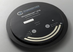
CyberOptics to Demonstrate Final Version of WaferSense Airborne Particle Sensor

CyberOptics will be giving a demonstration of the final production version of the WaferSense Airborne Particle Sensor (APS) at Semicon, which will be held in Japan during 5 to 7 December.

Apart from the APS, CyberOptics will be giving a demonstration of the complete line of WaferSense wireless metrology devices at the international show.

The WaferSense APS provides superior performance when compared to the conventional static airborne particle sensors. The limitations of the conventional sensors such as the static output and limited reach are eliminated with the WaferSense APS. The APS goes through the entire semiconductor process for counting and identification of the particles real time. The semiconductor process in APS minimises the time and also the expense related to the particle identification process. Using the APS for airborne particle identification improves the die yield and also the final wafer inspection process. Fabs are provided for isolating and mitigating the source of the particles by using a tool before the wafer processing begins. The sensor is used to identify and classify the air particles along with their sources while the wafers are transferred, split valves actuate and cycling, flushing out and pumping of chambers.

Read More