by Shou-Nan Li, Hui-Ya Shih, Shaw-Yi Yen, ITRI; Kan Hsieh, Winbond Electronics Corp.; Jean Yang, TPO Displays Corp.
September 15, 2009 – Airborne molecular contaminants (AMC) pose tremendous yield threats to hi-tech industries because an AMC of a concentration from ppt (part per trillion, 10-12) to ppb (part per billion, 10-9) level could seriously damage electronic devices. So to maintain a high yield, AMC-related information and technology should be shared and learned quickly. In this study, five AMC control cases from a semiconductor fab as well as a TFT-LCD fab are presented. By sharing the case scenarios and their follow-up mitigation measures, it is expected that similar micro-contamination problems could be avoided and the product yield be enhanced.
Five case studies were examined:
- Stack NH3 emissions of 108ppm (parts per million, 10-6) contributing to exceptionally high NH3 concentration of 57ppb at the make-up air unit (MAU);
- Acid gases (e.g., HBr, HCl, HF, SiF4) at a ppm level continuously outgassing from newly dry-etched wafers for 30 minutes;
- Etching gases (CF4, CHF3, Cl2, HBr, HCl, SF6) of several hundred ppm leaking from an exhaust pipeline;
- Fine NH4NO3 particles blurring optical lens due to continuous NH3 emission during the maintenance activity of a photo-resist stripper in a thin-film-transistor liquid-crystal-display (TFT-LCD) fab;
- Re-entrained boron cross-contaminating the glass substrates inside an LCD stocker.
In addition to the lessons learned by sharing this data, it is expected that similar micro-contamination problems could be avoided and the product yield be enhanced. New monitoring and cleaning technologies for micro-contamination might also be developed based on the results of this study. It is also shown that some AMC problems in a semiconductor fab could occur in a TFT-LCD fab, such as lens hazing (caused by fine [e.g., salt] particles).
Background on AMCs
Airborne molecular contaminants (AMCs) in five different categories render distinct defects on an electronic device [1]. For example, molecular acid (MA) causes corrosion problem [2]; molecular base (MB) induces T-topping damage [3]; molecular condensables (MC) change the deposited film property from Si-N to Si-O [4] and haze the photo lens [5]; molecular dopant (MD) shifts the p-type and n-type properties [6]; ozone (O3) lowers the device capacitance [7]. Particles larger than 1/3 of the feature size might fail a die [8]. To reduce the wafer losses resulting from AMCs, the yield enhancement committee of the International Technology Roadmap for Semiconductors (ITRS) annually publishes a guideline to detail the tolerable concentrations for various AMCs in each technology node [9]. For instance, since the 65nm process, ITRS has been recommending that the dopant (chemical containing As, P, B) concentration in the wafer environment be less than 10ppt.
In theory, the best strategy to control the contaminants is to locate the emitting origin and terminate the releasing source. In a cleanroom, the contaminants mainly originate from two sources: a) incoming outdoor air at the make-up air unit (MAU), and b) internal activities (e.g., maintenance activity, wafer outgassing). For the incoming outdoor air, as long as the contaminants are identified, a combination of particle and chemical filter can effectively remove the contaminants [10].
However, for the contaminants released by internal activities, the contaminating chemicals could easily damage the electronic device due to proximity and localized high concentration. Therefore, huge product losses generally result from internally generated contaminants. Based on the literature, the internal contaminants could come from several sources: MA and particles from preventive maintenance (PM) activities [11], MB from neighboring chemical mechanical polishing (CMP) and photo-resist stripper areas [12], MC from plastic utilities (e.g., wafer cassette, gloves) [13], MD from glass fiber filter [14] and filter sealant [6], O3 from a O3-water mixing chamber [15], particles from persons, garments and wipers [8, 16]. Besides the referenced cases in this study, five additional AMC events and their mitigation experiences are shared, which are expected to help the IC/LCD industries reduce yield losses and AMC mitigation costs.
Materials and methods
The instruments and methods used to determine various AMC compositions are shown in the Table below. A movable closed-cell (CC) Fourier transform infrared (FTIR) spectrometer with a 10m optical path length was used to instantly identify and quantify the gases from point sources [11], such as those from stack emissions, PM activities and outgassing wafers. To identify the wafer outgases, a compressed clean air flow of 3 L/min was used to purge the enclosed wafer cassette and transfer the gases to the FTIR. An open-path (OP) FTIR was employed to determine the line-average (NH3) concentration along the MAU. To locate the leaking spot among thousands of gas pipelines, a gas-leaking-detection-system (GLDS), composed of two open-path FTIRs, a gas composition database and diagnostic software, was applied [17].
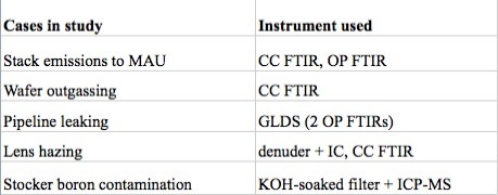 |
| Sampling and analysis instruments used in different AMC cases. |
For optical lens hazing investigation, a personal porous-metal denuder [18] was applied to take the air samples inside the blurred optical equipment (193nm) for two hours. After the sampling, the chemically impregnated, porous metal disks were carefully sent back to the laboratory, extracted by distilled, deionized water (DDW) and then analyzed by an ion chromatography (IC) (ICS-90, Dionex, CA USA).
For the boron contamination investigation, the air samples inside and outside three suspected stockers were simultaneously taken by using KOH-impregnated cellulose filters [19] for 48 hours at a sampling flow rate of 10 L/min. The used 47mm cellulose filters were extracted by a 10mL DDW solution added with 2 M HCl (~100μL) and analyzed by an inductively coupled plasma/mass spectrometer (ICP/MS) (7500s, Agilent Technologies). After the air sample analysis, it was found that only in one LCD stocker the inside boron concentration was higher than the outside one. This meant that there was a contaminating source inside this stocker. To trace the contamination origin, the stainless-steel frames of this stocker were wiped by the KOH-soaked Teflon filters. The wiping area for each frame was fixed at 0.1 × 0.1m. The wipe samples were then extracted by DDW-HCl solution and analyzed by an ICP/MS.
Results and discussion
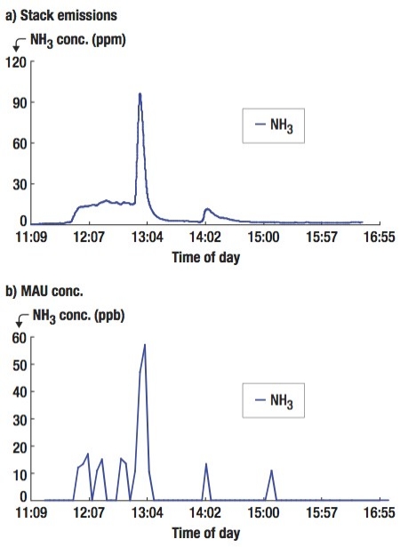 |
| Figure 1. NH3 concentrations a) inside a stack emissions, and b) entering the MAU. |
To ensure the stack-MAU relationship, a pure tracer SF6 flow of 50 L/min was intentionally released into the stack for 10 minutes. It was measured that ~0.5% of the tracer gas would enter the MAU. If not properly controlled, the incoming NH3 would render various defects, such as T-topping and lens hazing, and the costs of NH3 mitigation measures (e.g., chemical filters) would greatly increase. To mitigate the NH3 emissions from the stack, by following the SEMI-F5 guideline, the pH value of the scrubbing water was maintained at ~4 all the time and the NH3 emission concentration was then greatly reduced to <1ppm.
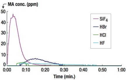 |
| Figure 2. Outgassing MA concentration variations from a batch of newly dry etched wafers (#25). |
To prevent the MAs from causing defects, a well-vented storage cabinet was constructed at 1.4 × 1.5 × 0.75m with internal circulation air flow rate equal to 4200 L/min. Based on the findings of this study, the newly dry-etched wafers were temporarily arranged inside the cabinet for 30 minutes to diffuse out the MAs before being sent to the next process equipment. With this arrangement, the effect of throughput losses can be minimized.
By effectively controlling the acid gas emissions, the contaminating particle counts on the wafers were significantly reduced [15]. This is because the MAs react with the MBs (e.g., NH3, amines) present in the cleanroom to form fine salt particles [21]. Due to closeness, the in situ generated fine particles could easily deposit on the wafer surface and cause device defects. However, when the MAs were drawn away from the wafer surface, the number of chemically-generated fine salt particles would be greatly reduced, which resulted in the decrease of particle counts on the wafers.
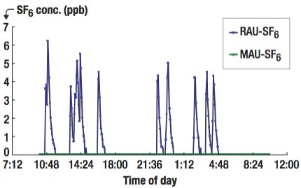 |
| Figure 3. Measured SF6 concentrations at the RAU (blue lines) and at the MAU (green lines) by two OP-FTIRs. |
To find the emission source, an extractive FTIR was used to measure the air quality around a suspected photo-resist stripper during its preventive maintenance (PM) activity. As Figure 4 shows, high concentration of NH3 was continuously emitted into the cleanroom during the PM of the photo-resist stripper, which used mono-ethanol-amine (MEA) as its stripping chemical. The three photos shown on the top of Fig. 4 represent NH3 emissions from used wiping cloth (left), from the gap around the chamber door rim (middle) and from the activities of cleaning the chamber inner surfaces (right). To control the NH3 emission, air-tight chamber lids were applied around the rims of the process tool and distilled-water flush steps were added to reduce residual chemicals condensed on the internal walls. For the potential HNO3 (or similar chemical) source, unfortunately, its emitting origin was not found.
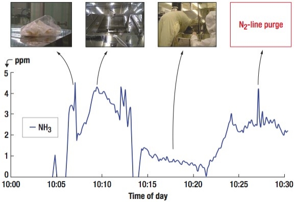 |
| Figure 4. Fugitive NH3 emissions in the PM activity of an LCD stripper, which uses mono-ethanol-amine (MEA) as its stripping chemical. |
When the glass substrates were stored inside the stocker to wait for the next process equipment, they were contaminated by the boron emitting from the surfaces of the stainless-steel frames. The boron on the frames could originally come from the fugitive emissions of the glass substrates. With long-time (~1 year) accumulation, the boron quantity on the frames became significant and detrimental to the LCD products although the boron emission from each glass substrate was insignificant. To resolve the boron contamination problem inside the LCD stocker, it was recommended that the stainless-steel frames be cleaned periodically (~once per month) with KOH-DDW solution to avoid significant boron accumulation.
Conclusion
Locating the contamination source and then mitigating the releasing origin proves to be an effective way to tackle airborne molecular contamination (AMC) problems. For example, by mitigating the stack and PM NH3 emissions, NH3-induced defects and chemical filter costs can be minimized; by controlling the MA-releasing wafers, similarly, corrosion-related defects and equipment damages can be reduced. To pinpoint a leaking spot among thousands of gas pipelines, the GLDS demonstrates its quickness and effectiveness. Additionally, a personal porous metal denuder demonstrated to be a useful tool to sample trace amount of MAs, MBs and particles; chemical-impregnated filters appeared useful for collecting the surface contaminants. After finding the contamination sources, based on cleanroom situations, different mitigation measures were then adopted. The results and experiences found in this study would be useful and beneficial for solving various contamination problems that originate from dynamic high-tech manufacturing processes and their demanding requirement on cleanroom air quality.
BIOGRAPHIES
Shou-Nan Li received his PhD from University of Florida and is a department manager at Energy and Environment Research Laboratories, Industrial Technology Research Institute (ITRI), 11F, Bldg. 51, 195-10 Sec. 4 Chung-Hsing Rd., Chutung, Hsinchu, Taiwan 310, R.O.C.; e-mail [email protected].
Hui-Ya Shih received her masters degree from National Chiao-Tung University (Taiwan) and is a researcher at ITRI.
Shaw-Yi Yen received her masters degree from National Cheng-Kung University (Taiwan) and is a researcher at ITRI.
Kan Hsieh received his masters degree from National Tsing-Hua University and is an ESH director at Winbond Electronics Corp., Taiwan, R.O.C.
Jean Yang received her masters degree from National Tsing-Hua University and is a risk & ESH director at TPO Displays Corp., Taiwan, R.O.C.
References
1. [1] C.R. Ayre, A.K. Mittal, J.F. O’sullivan, "The Influence and Measurement of Airborne Molecular Contaminants in Advanced Semiconductor Processing," Semiconductor Fabtech, 24th Edition, 2005.
2. [2] J.K. Higley, M.A. Joffe, "Airborne Molecular Contamination: Cleanroom Control Strategies," Solid State Technology, pp. 211-214, July 1996.
3. [3] D. Ruede, M. Ercken, T. Borgers, "The Impact of Airborne Molecular Base on DUV Photoresists," Solid State Technology, pp. 63-70, Aug. 2001.
4. [4] K. Saga, T. Hattori, "Influence of Surface Organic Contamination on the Incubation Time in Low-Pressure Chemical Vapor Deposition," Jour. of the Electrochemical Soc., 144 (9), pp. L253-L255, Sept. 1997.
5. [5] S. Barzaghi, A. Pilenga, G. Vergani, S. Guadagnuolo, S Getters, "Purged Gas Purification for Contamination Control of DUV Stepper Lenses," Solid State Technology, pp. 99-104, Sept. 2001.
6. [6] J.A. Lebens, W.C. McColgin, J.B. Russell, E.J. Mori, L.W. Shive, "Unintentional Doping of Wafers Due to Organophosphates in the Clean Room Ambient," Jour. of the Electrochemical Soc., 143 (9), pp. 2906-2909, Sept. 1996.
7. [7] Y.K. Park, H.J. Kim, D.W. Kim, J.H. Park, "Environmental Ozone Effect on the Growth of Hemispherical Grained Silicon for ULSI DRAM Stacked Capacitor," Jour. of the Electrochemical Soc., 148 (8), pp. F170-F174, 2001.
8. [8] H. Kitajima, Y. Shiramizu, "Requirement for Contamination Control in the Gigabit Era," IEEE Trans. on Semiconductor Mfg, 10(2), pp. 267-272, May 1997.
9. [9] International Technology Roadmap for Semiconductors (ITRS), Yield Enhancement, pp. 28-34, 2007.
10. [10] C.F. Yeh, C.W. Hsiao, S.J. Lin, C.M. Hsieh, T. Kusumi, H. Aomi, et al., "The Removal of Airborne Molecular Contamination in Cleanroom Using PTFE and Chemical Filters," IEEE Trans. on Semiconductor Mfg., 17(2), pp. 214-220, May 2004.
11. [11] S.N. Li, H.Y. Shih, K.S. Wang, K. Hsieh, Y.Y. Chen, Y.Y. Chen, et. al., "Preventive Maintenance Measures for Contamination Control," Solid State Technology, pp. 53-56, Dec. 2005.
12. [12] B. Demandante, K. Murray, M. Alexander, "Protect DUV Processes with Real-time Molecular Monitoring," Semiconductor International, September 2000.
13. [13] K. Saga, J. Hattori, "Identification and Removal of Trace Organic Contamination on Silicon Wafers Stored in Plastic Boxes," Jour. of the Electrochemical Soc., 143(10), pp. 3279-3284, Oct. 1996.
14. [14] F.A. Stevie , E.P. Martin, P.M. Kahora, J.T. Cargo, A.K. Nanda, A.S. Harrus, A.J. Muller and H.W. Krautter, "Boron contamination of surfaces in silicon microelectronics processing: characterization and causes," J. Vac. Sci. Technol., A9 (5), pp. 2813-2816, Sep/Oct 1991.
15. [15] S.N. Li, Y.Y. Chen, H.Y. Shih, J.L. Hong, "Using an Extractive Fourier Transform Infrared (FTIR) Spectrometer for Improving Cleanroom Air Quality in a Semiconductor Manufacturing Plant," American Industrial Hygiene Assoc. Jour., pp. 408-414, May/June 2003.
16. [16] D.S. Ensor, J.M. Elion, J. Eudy, "The Size Distribution of Particles Released by Garments During Helmke Drum Tests," J. of the IEST, 44(4), pp. 24-27, Fall 2001.
17. [17] S.N. Li, G.H. Leu, Y.S. Yen, S.F. Chiou, K.S. Wang, S.J. Yu, et al., "Controlling Contaminants with Enhanced Gas Leak Detection," Solid State Technology, pp. 89-92, July 2007.
18. [18] C.J. Tsai, C.H. Huang, S.H. Wang, T.S. Shih, "Personal Porous-Metal Denuder," Aerosol Science & Technology (35), pp. 611-616, 2001.
19. [19] T.R. Fogg, R.A. Duce, J.L. Fasching, "Sampling and Determination of Boron in the Atmosphere," Anal. Chem. (55), pp. 2179-2184, 1983.
20. [20] L.L. Tseng, "Analysis and Effects of Acids and Bases Airborne Contaminants in Cleanroom on the Defects of Wafer Devices," Masters Thesis, Yuan Ze U., pp. 119-122, 2007.
21. [21] K. Kanzawa, J. Kitano, "A Semiconductor Device Manufacturer’s Efforts for Controlling and Evaluating Atmospheric Pollution," IEEE/SEMI Adv. Semiconductor Mfg. Conf., pp. 190-193, 1995.
22. [22] E.V. Johnstone, C. Chovino, J. Reyes, L. Dieu, "Haze Control: Reticle/Environment Interactions at 193nm," Solid State Technology, pp. 69-73, May 2004.

