by Debra Vogler, senior technical editor, Solid State Technology
As the semiconductor equipment industry looks ahead to what it hopes will be a much better economic picture going forward than in the past year or so, Ultratech’s chairman/CEO/president, Art Zafiropoulo, updated SST on the company’s strategy and focus.
Last year, Zafiropoulo alluded to an alpha tool with which customers were characterizing melt laser spike anneal (LSA) technology. Today, customers are still evaluating melt technology at 22nm, 16nm and even sub-16nm nodes, he notes. "When they establish the [process] conditions, we’ll start to manufacture the actual production melt system," he said. Ultratech still expects a transition from sub-melt LSA to melt LSA at around 22nm with more emphasis placed on melt technology at 16nm.
Regarding investment and industry readiness, Zafiropoulo acknowledged that the company didn’t fully appreciate the significance of the downturn in 2009. Because of the time delay given the economy, he expects there to be less investment in 65nm and more in 40/45nm as well as 32nm as the industry reestablishes its footing. "There will be a slight improvement in memory and selectively, in logic at 32nm and 22nm, but there is still not a great deal of production at 40/45nm," he noted. The bulk of the major logic manufacturers are still developing 40/45nm technology and are not yet in full production, but rather pilot production, he added.
Jeff Hebb, Ultratech’s VP of marketing for laser processing technology, focused on the advantages of LSA technology to address leakage issues at July’s AVS West Coast Junction Technology Group Meeting. Last year, addressing the same audience, Hebb presented data showing the extendibility/compatibility of LSA with 32nm, including HK+MG. "We still believe that LSA technology is also extendible to 22nm," Hebb told SST. Between last year and this year, end users have been trying to refine their 40/45nm and 32nm processes, and the issue of leakage has worsened. Because mobile applications (e.g., smart phones, netbooks) require both high performance and low leakage, the dual requirements are proving to be serious challenges that have to be met simultaneously.
LSA can go to higher process temperatures that increase junction activation — forming more abrupt junctions — so leakage is lowered. The higher process temperatures are possible because only a very thin surface layer of the wafer (where the transistors are formed) is heated. Furthermore, dwell times (at elevated temperature) are very short; annealing times can be on the order of milliseconds, microseconds, or, at the melt condition, nanoseconds. And while HK+MG itself reduces leakage by a factor of ~10×, "LSA provides extra leakage reduction that is additive, so you get an additional 3×-5× reduction in leakage [on top of the leakage reduction with HK+MG]," Hebb told SST.
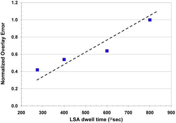
Another major concern at advanced nodes is lithography overlay error. Hebb explained that because LSA is able to keep stress in the wafer low — only a small portion of the wafer at any given time is heated and the dwell time is short — it is able to meet the ever more stringent lithography overlay error requirement (see Figure). And when the industry is ready to move to FinFET structures, LSA is extendible. "We think millisecond annealing tools will be challenged to deal with FinFETs," said Hebb. — D.V.
 |
| Normalized overlay errors for 32nm device wafers vs. LSA dwell time. Reducing the dwell time from 800μsec to 275μsec reduced overlay errors by 60%. (Source: Ultratech) |

