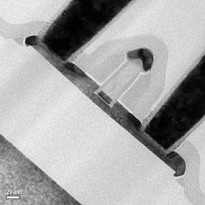
October 21, 2009 – French R&D organization Leti says its work with SOI-based planar CMOS meets requirements for low-power (LP) 22nm node device requirements, e.g. consumer electronic devices such as 4G mobile phones.
 |
| High-k/single metal gate technology on SOI using selective epitaxy process without channel doping and no pocket. Gate length = 25nm. (Source: Leti) |
Among the results touted:
— A factor-of-two reduction in variability on threshold voltage vs. FinFET technologies at both wafer and batch levels. Variability is a major challenge at 22nm; the result also proves that such control is possible with wafers available today.
– Less than 100mV/V drain-induced barrier lowering
– Enable reduction of electrostatic parasitics
– Scalability down to 10nm for fully depleted SOI CMOS, by tuning buried oxide and silicon layer thickness; FDSOI also addresses variability issues for this shrink.
Leti says planar technologies are superior to other transistor architectures based on bulk CMOS and FinFET architectures, offering faster and easier transition to 22nm node manufacturing, according to Leti CEO Laurent Malier, in a statement. "We have demonstrated that planar SOI dramatically improves the energy performances of many products that will change our lives, while offering long-term success for many companies involved in these fast-growing markets," he said.
This follows recent news that a 45nm high-power test chip offers 40% power savings vs. a bulk LP process.

