October 26, 2009 – Researchers from SEMATECH have developed a new way to model transistor noise that can help extract defect characteristics from low-frequency noise data in advanced gate stack transistors with conventional and novel dielectrics, seen as a key step in defect analysis and elimination needed for device scaling.
Low-frequency noise — random fluctuations in device current, caused by electrons jumping back and forth from the substrate into a defect in the dielectric — is of increasing concern as CMOS is scaled ever further. Conventional modeling for such noise, based on "elastic tunneling," looks at the time of an injected electron capture by a bulk defect as controlled by the tunneling process. Unfortunately, this has been shown by NIST researchers to not work as predicted, and the SEMATECH researchers agree, saying the measured characteristic times are "several orders of magnitude longer than the estimates based on the tunneling times," with carrier capture rates can be off by a factor of 1000× or more.
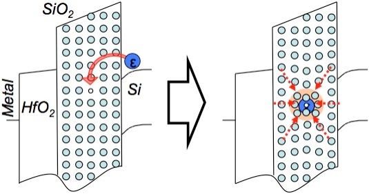
The new work, reported at the IEEE’s recent Integrated Reliability Workshop (IRW), instead turns to the concept of "lattice relaxation" around a defect — when a defect traps an electron the neighboring nuclei "feel" it and shift positions (i.e., "relax") to accommodate the new force; this requires a certain amount of energy, which amounts to a barrier that slows the rate of charge capture, SEMATECH notes in a statement. "The times of capture and emission by the bulk oxide traps might be controlled to a great degree by the trap structural relaxation rather than by electron tunneling," the researchers noted in their paper abstract.
 |
| Schematic representation of the electron trapping process: relaxation caused by the trapped charge involves displacements of the lattice atoms around the defect. The energy barrier associated with the motion of the atoms around the defect is responsible for slowing down the trapping/de-trapping process significantly increasing electronic capture and emission times. (Image courtesy of SEMATECH) |
Using their proposed methodology, the researchers said they were able to extract characteristics of defects in high-k/metal-gate (HK+MG) and SiON/poly-Si transistors, and in the tunnel oxide of the charge trapping memory devices (TANOS).
"To optimize noise performance in various applications, we need to be able to accurately simulate the processes responsible for noise," said Gennadi Bersuker, project manager of electrical characterization and reliability at SEMATECH and one of the paper’s authors, in a statement. "With the proposed model, the reliability community now has a means of identifying the atomic structure of the defects, allowing feedback to process and integration groups to facilitate reduction and elimination of the defects."
"The SEMATECH work explains several orders of magnitude difference between older, so-called, tunneling models and the noise measured in advanced CMOS with ultrathin oxide layers," added Michael Shur, professor at Rensselaer Polytechnic Institute.

