by Debra Vogler, senior technical editor, Solid State Technology
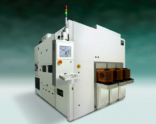
November 2, 2009 – Novellus Systems recently introduced its Sabre Excel, an advanced copper electroplating system designed to provide fill and defect density performance for the 22nm technology node and beyond. The new technology builds upon the company’s Sabre platform.
To address device reliability concerns associated with copper electroplating at the 22nm node, the industry is trending towards the use of very thin alloy PVD seed layers, explained Sesha Varadarajan, VP & GM of Novellus’ electrofill business unit. While thicker PVD seed layers can cause copper voiding, thinner seed layers result in increased seed resistance, making it difficult to achieve the uniform current density required for consistent feature fill during the initial stages of electrochemical deposition (ECD). According to Varadarajan, the company’s new IRISCell technology eliminates this issue by employing patented field shaping elements that enable dynamic current modulation during the deposition process. To ensure a uniform fill process, the electrons have to be distributed equally because the fill process is so sensitive to the current density. "We invented a cell that has focusing elements to distribute the current uniformly preventing edge bias that can narrow, or sometimes eliminate, the window you might have in which a good fill can happen," Varadarajan said.
Thin PVD seeds also create a challenge for uniform nucleation of the copper film. To address this problem, Novellus developed a new "Multiwave" plating process that provides millisecond control of the voltage profile during the initial stages of copper deposition. Millisecond control is "old hat" for vacuum processes, Varadarajan acknowledged, but for plating it is a leading-edge technology. "Many factors affect the filling process, including absorption and desorption of plating additives from the wafer surface" — proprietary additives in the electrolyte solution that modulate how the fill happens at various points on the wafer, said Varadarajan. "These additives have a time constant associated with absorption/desorption, so there is no benefit to having voltage control that exceeds the time it takes for the additive to come into play. So millisecond control represents state-of-the-art."
Controlling the growth early in the process is crucial, noted Varadarajan; an initial nonuniformity in nucleation can be propagated such that growth occurs preferentially in one location vs. another. "We are avoiding the problem of nonuniform growth within a feature by dynamically controlling the voltage to a precise amount," he said. "Once the process is established and the growth front is happening, the additive concentration is influenced by how long the process has happened — that ends up taking over control, so microscopic control of the field is not so important." Thus, millisecond control is sufficient for the fill process.
 |
| Figure caption: Comparison of traditional "wet" contact (a) vs. Novellus’ dry, sealed contact (b). Plating on contacts can cause defects at small edge exclusion; eliminating plating closes contacts, enabling 1mm edge exclusion process. (Source: Novellus Systems) |
Other features of the new system include the use of a proprietary low-corrosion electrolyte that the company says reduces the propensity for killer defects; and reducing the process edge exclusion to only 1mm, which increases the usable die area and thus the number of chips per wafer. Changes made to the wafer holding apparatus that reduce the edge exclusion include a much lower profile, and the use of exotic materials to handle the strength requirements of the clamping, according to Varadarajan. He pointed out that Novellus’ sealed contact technology excludes the backside and a frontside corner of the wafer from the electrolyte, so only the face of the wafer actually sees the liquid. "Within this dry space, we have electrical contacts to pass the current," he said.
Looking ahead to 16nm, Varadarajan explained that while there is no patterning capability to prove that 16nm can be achieved in a broad sense, from a damascene standpoint the company believes that the smallest geometry that will probably be seen is on the order of 1.5× the node (varying among end-users) — e.g., for the 22nm node, aggressive features are on the order of 28nm, unlike the contacts which will be at design rule. Thus, the company projects that its validated filling capabilities on extremely small trenches (22-23nm) are roughly the dimensions that will be seen on a 16nm logic device. "We believe the fill capabilities we designed into the system have some legs to carry us to a node beyond 22nm," Varadarajan predicted.


