by John Klawender and Terry Bluck, Intevac
EXECUTIVE OVERVIEW
Historically, semiconductor OEMs have developed, manufactured, and marketed semiconductor equipment as a unit, typically including a platform and process module(s). However, the main focus of equipment manufacturers is in the development of next-generation process modules while making minimal efforts in platform and performance innovation. Now, the necessity for a forward thinking, flexible platform is recognized as a vital element in order to meet the cost and productivity challenges of 450mm and beyond. Accelerating cost reduction for chip manufacturers demands an infrastructure change in the semiconductor equipment supply model that can only begin when OEMs commit to the development of a common platform and a common standard. The following paper presents the concept and capabilities of a universal platform and the results that were achieved through testing and system modeling.
December 28, 2009 – The worldwide semiconductor industry is now faced with the urgent challenges presented by the increased pace of IC development mandated by the International Technology Roadmap for Semiconductors (ITRS) and Moore’s Law. As we prepare for the transition from 300mm to 450mm, the International SEMATECH Manufacturing Initiative (ISMI) is developing standards to help equipment and IC manufacturers achieve an expedient, successful and rapid conversion. With the industry actively striving to implement innovative solutions to accelerate the next transition, reduce costs and improve the quality and productivity of chip manufacturing, the concept of platform interoperability has been clearly identified as a crucial element in equipment redesign.
Aligning with ISMI’s proposed roadmap to 450mm and the need for platform interoperability expressed by the world’s top IC manufacturers during ISMI’s October 2009 platform meeting, a breakthrough solution for the development of a universal platform was introduced. The new mainframe platform architecture, combined with a new wafer transfer system, will ultimately accelerate cost reduction, improve throughput, wafer processes and quality, and free equipment manufacturers to concentrate on developing next generation module and chamber technologies. A universal platform offers the capabilities necessary to meet the ongoing changes in design nodes and increasing wafer size.
Candidate for a standard solution
A common standard solution goes beyond establishing the standard interface for platform interoperability. Combining a new platform concept and design with a platform standard can produce significant benefits that can be realized by both chip and equipment manufacturers. Today’s platform and wafer transfer systems are mostly constrained by and limited to ‘chamber reach robot’ design with only rotational motion. To enable flexibility and maximize productivity, multiple robots must be used on individual platform units. This relay model commonly used in 300mm has reached its limit and no longer has the ability to enable a common standard approach that will benefit 450mm manufacturing.
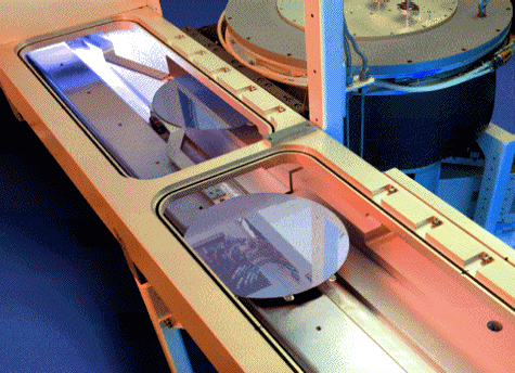 |
| Figure 1. Decoupled linear dual robots used in the universal platform design. |
A platform with linear motion architecture is designed and developed to deliver a flexible, economical solution that enables the flexibility necessary to increase productivity. The new platform architecture (referred to as the universal platform in this paper) and wafer transport designs are shown in Figures 1 and 2. The universal platform is configured as an independent and self-functioning system, with mechanical, electrical, and software interface components. The universal platform allows friendly, hand-shake protocol and the ability to ensure platform interoperability. The compact design allows for easy expansion and chamber addition while minimizing the floor space needed. This design also enables the flexibility necessary for best-of-breed process chamber adoption.
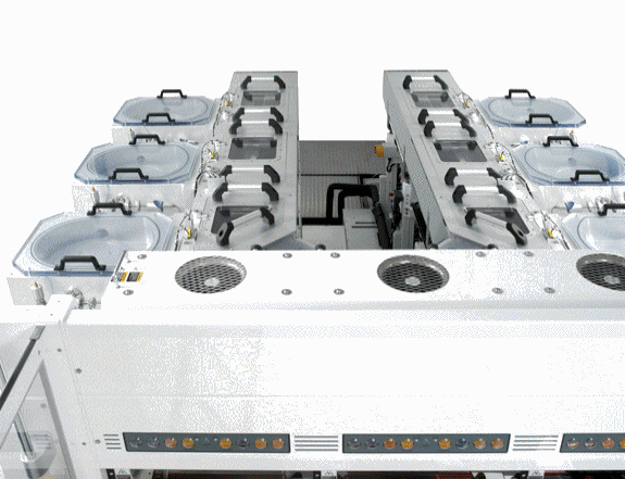 |
| Figure 2. The universal platform in dual transfer module configuration. |
The universal platform consists of the mainframe, (also known as the platform in the equipment application), and provides all the handling capabilities between the equipment front-end module (EFEM) and the process modules or chambers. The mainframe consists of the load lock (LL) and the transfer module (TM). The LL has two substrate or wafer slots and serves as a process material exchange point between the atmospheric EFEM and the TM. The TM is designed with a mechanical interface connecting to multiple chambers, which are arranged in linear fashion. The TM uses linear dual robots equipped with a dual arm set. Each robot arm has a single blade for wafer transport. Both robot arms travel linearly inside the TM, guided by a liner track. Both robot arms are decoupled for completely independent operation, and are designed for optimized wafer exchange at a pick up/place station with dynamic wafer transfer algorithm, (a high speed signal processing system combined with a synchronized operational code for real time optimization and wafer swap strategy) and for high throughput performance.
The universal platform can be structured in different configurations, e.g., in single TM mode or parallel TM mode (Fig. 2). Single TM mode is configured with one mainframe, including one LL and one TM, connecting to a single EFEM. Parallel TM mode is configured by pairing two mainframes, each including one LL and one TM, to a single EFEM, with an optional vacuum wafer transfer station that connects the pairing TMs. In contrast to today’s conventional robot and platform concept, the universal platform is designed to allow multiple chambers to be configured on the same mainframe without adding additional robots.
Throughput modeling
To compare platform and wafer transport advantages, several throughput models and calculations were carried out based on the universal platform architecture, with different robot transport designs to mimic the semiconductor wafer manufacturing process sequence, including dual robots (for the universal platform design shown in Fig. 1 above), single-blade robot, single robot with dual blades (also referred as a double-bladed robot in the modeling).
The throughput model and calculation is based on the following assumptions and established model by M. Pinedo [1] and Perkinson et al. [2].
The LL is infinitely fast, and the wafers are always available for pick up.
- Pick up time from a chamber is the same as drop-off time to a chamber. Pick up time is referred to as "T."
- The time "T" is the same for every chamber as well as for the LL.
- The time to move between any two chambers is constant (since it depends on the system configuration and cannot be predicted here). This time is regarded as an average time to move between the chambers.
- The process job for all the wafers is the same — any given chamber will have an identical process time for every wafer visiting it.
- The system is running in a steady state.
Furthermore, in order for a meaningful comparison, conservative approximations of the hardware speeds are made. Most notably:
- A chamber pick up time (T) is assumed to be 5 seconds.
- Fast rotation time (without wafer) is assumed to be 0.25 seconds.
- Slow rotation time (with a wafer) is assumed to be 2 seconds.
- Fast linear move (without a wafer) is assumed to be 2 seconds.
Once a system has been fully populated with wafers, it is deemed to be working in a steady state. Perkinson et al., described this steady state as follows: "…where the inflow of a new wafer into the system and the outflow of the processed wafer from the system are equal." Throughout this paper we will be dealing exclusively with the steady state conditions.
Perkinson et al., also introduced the concept of the fundamental period and defined it as: "…the time between subsequent completed wafers arriving at the load lock." Later in this paper, it will be evident that robot speed, chamber process time, number of chambers in the wafer flow and the number of blades on the robot will all affect the fundamental period.
The inverse of the fundamental period is the measure of the number of wafers processed on a system within a unit of time, and it represents the throughput of the system.
Consider a simple serial processing on M chambers, where a wafer flow is given as:
and assume that the process times in all the chambers are the same, i.e.:
Once all the wafers have finished the processing step, the robot needs to advance them to the consecutive chambers, i.e., the wafer in the chamber mM is shifted out to the LL, the wafer in the chamber mM-1 is shifted to the chamber mM, the wafer from chamber m1 moves to chamber m2, and finally a new wafer is introduced into the system as it is being moved from LL to the chamber m1.
Let tboundary be the combined time the robot needs to shift all the wafers to the successive chambers during one advancement cycle. In the extreme case, when the process times in all the chambers are zero, the robot will start a new cycle immediately after it has finished the previous cycle. In fact, the same outcome will result for any process time >0, but shorter than tboundary. Such a system is deemed to be transfer bound and can be envisioned as a system where the robot is always busy, while the wafers are waiting for pick up in the idling chambers. Observe that the maximum throughput (μmax), obtainable by the machine (for a given set of chambers), can be achieved only in this region. The important consequences of working under the transfer bound region are:
- Maximum throughput can be reached;
- Process time does not affect the throughput;
- Chambers utilization is poor.
When the process time exceeds tboundary, the robot will have to wait during each advancement cycle for the chambers to finish processing. In these settings, the system is deemed to be working in the process bound region. As the process time increases, the following results are noted:
- Robot utilization decreases.
- Chamber utilization increases.
- Throughput decreases.
Note that the elapsed time between the starting times of two consecutive cycles is the same as the elapsed time between subsequent wafers returning back to the LL, which can be also viewed as the fundamental period of the system.
Finally, the initial stipulation was that the process times in the chambers were equal. We will relax this requirement now and propose that only the sole chamber with the largest process time needs to be considered. This single chamber, described as the bottleneck (in the process bound region), is the only chamber that affects the throughput; the process times of all the other chambers are of no consequence (on the following pages we shall assume that all the chambers are bottlenecks).
Serial and parallel wafer processing
There are two commonly used process sequences in wafer fabrication in use with conventional vacuum equipment; serial and parallel processing. Serial processing is described next with throughput model for linear transport system.
In the serial processing model, wafers are transported to one or more chambers based on a given serial processing sequence. In all the cases analyzed, the wafer flow is: m1 → m2 → … → mM, and the processing times in all the chambers are assumed to be equal (t1 = t2 = …. = tM = tMAX).
Single blade robot. The "pull" strategy of advancing wafers with a single-bladed robot is illustrated below. This strategy has been devised by Perkinson et al., and is considered to be optimal.
- Pick up a wafer from chamber mM, make a slow move to LL, and drop off the wafer.
- Make a fast move to chamber mM-1, pick up the resident wafer, make a slow move to the chamber mM and drop off the wafer.
- Continue in this fashion until the wafer from chamber m1 is moved to chamber m2.
- Complete the cycle by picking up a new wafer from LL, making a slow move to chamber m1 and dropping off the wafer.
The process times were set to match the boundary condition, i.e., the new movement cycle starts immediately when the previous cycle is completed, and each wafer is picked up as soon as it is finished processing. The sum of the times associated with all robot actions during one movement cycle is the fundamental period for the transfer bound region and, as can be seen on the diagram, is given by:
By extending the process time in any of the chambers, the system will enter the process bound region. The fundamental period will be a composition of the process time and the time needed to perform one wafer swap.
By equating the above equations, the boundary between the regions can be established:
Double bladed robot. This is the robot system where the two blades are incapable of making individual, decoupled rotary moves. We assume that both blades always face the same direction. The equations given would be analogous if the blades were rotated with respect to each other.
An optimal "swap" strategy for double bladed robot is given in Venkatesh et al. [3].
- Pick up a wafer from the LL with one blade.
- Rotate slowly to face chamber m1, pick up the resident wafer with the empty blade and replace it with the wafer acquired from LL.
- Rotate slowly to face chamber m2, pick up the resident wafer with the empty blade and replace it with the wafer acquired from chamber m1.
- Continue in this fashion until all the chambers have been swapped.
- Complete the cycle by slowly rotating from chamber mM to LL, picking up a new wafer with the empty blade and dropping off the wafer picked up from chamber mM.
Transfer bound: FP = (M+1) (2T + tslow)
Process bound: FP = tmax + 2T
Tboundary = M (2T + tslow) + tslow
Dual robots. The decoupled linear robots (i.e., two individual robots based on the universal platform design, shown in Fig. 1 above) in a linear transfer module can perform individual tasks independent from each other, and thus have the potential to outperform the coupled robots or blades in more challenging scheduling problems (e.g., two different process jobs running simultaneously). For a simple serial processing scheduling problem, the swap strategy, as described above, can also deliver optimal operation by decoupled robots.
Process bound: FP = tmax + 2T
Tboundary = M (2T + tfast) + tfast
The modeling of linear dual robots is shown in the Figure 3 modeling comparison.
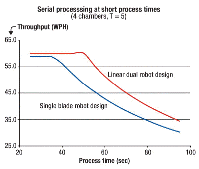 |
| Figure 3. Throughput comparison of single blade robot vs. dual robot design as function of process time, in serial processing mode, based on the universal platform. |
Effect of chamber addition
To further enhance the throughput for the linear dual robot system on the universal platform, the effect of chamber addition is investigated. Since the maximum throughput is achieved in the transfer bound region, and the fundamental period for the transfer bound region during serial processing is a function of the number of chambers used, it follows that by adding more serial chambers the fundamental period will increase in this region; therefore, the maximum attainable throughput will be increased, as seen in Figure 4.
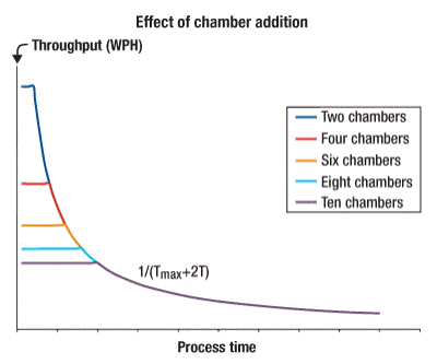 |
| Figure 4. Throughput comparison for different numbers of process chambers, for example M = 2, 4, 6, 8 and 10 chambers, for the linear dual robot design, in serial processing mode, based on the universal platform. |
Parallel TM mode
To further maximize the throughput for the system with a large number of chambers used in serial processing, utilization of parallel transfer chambers of the universal platform is demonstrated. For the universal platform with parallel TM mode (two mainframes: side A TM and side B TM, connecting to one EFEM, with optional wafer transfer station connecting the pairing mainframes), ideal configuration can be achieved. In an ideal chamber configuration, in terms of the number and position of the chamber(s), the robots in each transfer chamber need to service only half of the total load, thus reducing the transfer bound fundamental period, which virtually doubles the maximum throughput.
To derive the fundamental period for a system with parallel transfer modules the following assumptions were made:
- A wafer enters the system through the LL on Side A and leaves the system through the LL on Side B.
- There is an even number of process chambers on the system.
- For a wafer flow m1 → m2 → … → mM, the chambers m1 … mM/2 were placed on side A, while the chambers mM/2+1 … mM were placed on side B.
Process bound: FP = tmax + 2T
Tboundary = M/2 (2T + tfast) + tfast
Parallel TM configuration allows for a substantial maximum throughput improvement as can be observed in Figure 5. For jobs requiring fewer process steps, the unused positions can be used to multiply the number of the bottleneck, thus driving tmax down toward tboundary, and increasing the throughput in the process bound region. The significant advantage of this configuration is shown in Fig. 5.
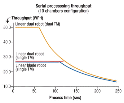 |
| Figure 5. The model compares single blade robot vs. linear dual robot design, and single vs dual TM configuration with linear dual robot design, based on the universal platform architecture. |
Actual wafer processing has been carried out to validate the modeling and performance of the linear dual robot system in serial processing mode on the universal platform. Modeling and wafer processing were also conducted for parallel processing mode based on different wafer transport design and architecture to mimic the semiconductor wafer manufacturing process sequence. In the parallel processing model, wafers are transported to only one chamber. Similar results were concluded comparing linear dual robots, single blade robot, and double-bladed robot. The results revealed the significant advantages of the universal platform design with the linear dual robot transport system over alternative wafer transfer designs used in the traditional cluster mainframe or relayed modular linear mainframe designs.
Conclusion
The linear dual robot design demonstrates an innovative solution and presents a challenge to traditional cluster platform and new modular platform architecture. The universal platform architecture brings true innovation to semiconductor equipment design and cost and productivity benefits to both equipment and IC manufacturers. The transition to 450mm presents an opportunity for the industry to consider an out-of-box platform approach and realize a win-win solution based on a common standard.
Biography
Janusz Klawender received his BS in computer science at Union College, Schenectady, N.Y., and is a member of the technical staff, software, at Intevac, 3560 Bassett Street, Santa Clara, CA 95054 USA; ph.: 408-588-2110; e-mail: [email protected].
Terry Bluck received his BS in physics at San Jose State U., San Jose, and is VP of engineering at Intevac; ph.: 408-246-2214; e-mail [email protected].
References
[1] M. Pinedo, Scheduling : Theory, Algorithms, and Systems, 2nd ed., Upper Saddle River, NJ: Prentice Hall, 2002.
[2] T. L. Perkinson, P. K. McLarty, R. S. Gyurcsik, R. K. Cavin III, "Single-Wafer Cluster Tool Performance: An Analysis of Throughput," IEEE Trans. Semiconductor Mfg., vol. 7, pp. 369-373, Aug. 1994.
[3] S. Venkatesh, R. Davenport, P. Foxhoven, and J. Nulman, "A Steady-State Throughput Analysis of Cluster Tools: Dual-Blade Versus Single-Blade Robots," IEEE Trans. Semiconductor Mfg., vol. 10, no. 4, pp. 418-424, 1997.

