by Pete Singer, editor-in-chief, Solid State Technology
December 9, 2009 – Intel has further advanced leading-edge transistor work that incorporates III-V materials in the channel region of silicon-based ICs, integrated with a high-k gate dielectric for reduced gate leakage. Although not expected to be in volume manufacturing until the 11nm node, in 2015 or 2017, channels with III-V material offer much higher mobilities compared to silicon. This, in turn, enables higher drive current and the possibility of lower threshold voltages, which could enable a 10× power reduction. The transistors reported by Intel work set new records: the 35nm gate length devices have the highest reported values of a drive current (0.28mA/μm) and peak transconductance (1350μS/μm). The work was reported at this week’s International Electron Devices Meeting (IEDM) in Baltimore.
GaAs-on-silicon was the focus on much research in the ’80s but abandoned to due problems with the mismatch between the silicon and GaAs crystalline lattice, which caused a significant number of dislocation defects at the interface of the two materials. In 2001, Motorola researchers thought they had solved the problem by using a strontium titanate buffer layer, but the devices produced reportedly suffered from poor performance.
Intel’s work began about five years ago, and "we’ve been working our way through a list of challenges ever since," said Mike Mayberry, director of components research and VP of Intel’s technology and manufacturing group. "We believe we can make it work now because we have new materials and processes, such as ALD." Many of the new material and deposition methods are already in use starting with 45nm node.
 |
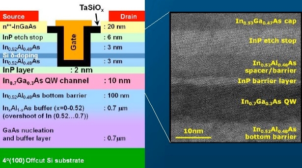
| Fabrication of QWFET with high-k. (Source: Intel) |
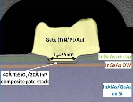
The work presented at this year’s IEDM is a quantum well field-effect transistor (QWFET), where 10 different layers are used between the silicon and the source/drain regions (see figure 1). Five of those layers were deposited by molecular beam epitaxy (MBE). A key aspect of the new work is that a high-k dielectric (TaSiO-InP) was used (see figure 2).
The first layer is GaAs, deposited directly on silicon. The lattice mismatch creates "lots of ugly looking things" and strain, Mayberry acknowledged, but an InAlAs buffer layer "soaks up the defects" and another overlying InAlAs bottom barrier layer is clear. He said the thicknesses of many of the layers need to be controlled "pretty precisely" from the bottom barrier to the top InAlAs. These layers were deposited by MBE, which is gives precise control over film thickness but is relatively slow. A volume manufacturing process would likely employ an alternative approach, such as ALD or MOCVD.
 |
| QFET with high-k on silicon. (Source: Intel) |
Since the feasibility of III-V on Si was first demonstrated by Intel in 2007, the company has demonstrated enhancement mode operation and a way to increase hole mobility in p-type devices using strain (see Mayberry’s article in the April 2009 issue of Solid State Technology: "Progress towards the merger of compound semiconductors and silicon").
Scalability compared to silicon devices remains unknown, although work has started on self-alignment process and alternative geometries, as well as modeling efforts at universities and internally at Intel, Mayberry said. "There is a lot of integration activity that is yet to come for this to work," he said. "That activity will ramp up in the next couple of years."
Other highlights of the work Intel presented at this year’s IEDM:
- The device was fabricated on a silicon wafer substrate, pointing toward eventual process synergy with existing silicon infrastructure
- Gate leakage for short channel devices was reduced by 1000× while achieving 33% reduction in electrical oxide thickness vs. Schottky barrier devices
- High mobility and effective velocity were demonstrated, comparable to devices grown on native III-V substrates without high-k integration
- Electrical oxide thickness (Toxe) was 2.2nm; 30% improvement in intrinsic device performance compared to silicon devices with Toxe of 1.2nm.

