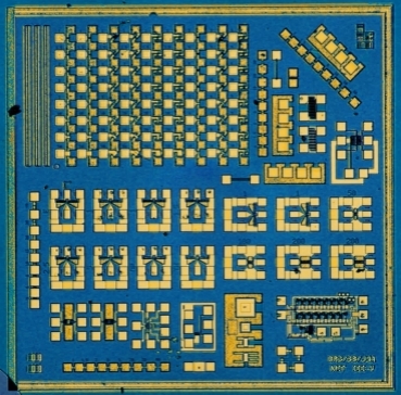
December 11, 2009 – Scientists at MIT’s Microsystems Technology Laboratories say they have built multiple transistors using III-V materials (in this case, InGaAs) with different gate lengths to figure out optimal conditions for making a logic element, and a pathway to make them smaller and better.
Two of their four papers presented at this week’s International Electron Devices Meeting (IEDM) updated work a year ago building a III-V transistor with record high-frequency operation, addressing properties of that transistor that better predict its performance as a logic element. They built chips with identical multiple transistors except for their gate lengths, and by comparing the chips’ performance at different frequencies were able to determine electron velocity through the transistor and electrostatic force exerted by the gate on the semiconductor layer.
The electron velocities they calculated, according to Jesús del Alamo, research team leader and MIT professor of electrical engineering, were "easily two and a half times higher than the best silicon transistors made today," and while the electrostatic force was lower than had been hoped (which del Alamo characterized as a "manageable problem"), the precision with which it was calculated will aid development of better physical models of III-transistors. While the MIT prototypes were built entirely with III-V materials, he envisions device structures incorporating "a silicon-like technology" (e.g. InGaAs) under the gate.
A third MIT paper presented at IEDM applied the team’s prototype measurements to work at Purdue, where simulators have been developed to model performance of even smaller III-V transistors. A fourth paper proposed a new design for III-V transistors that would work better at smaller scales by permitting a thinner layer of material to separate the gate and underlying semiconductor material, according to del Alamo.
 |
| A test chip used to evaluate the performance of indium gallium arsenide in logic circuits. (Source: MIT/the del Alamo group) |

