December 9, 2009 – At this week’s International Electronics Devices Meeting (IEDM) in Baltimore, Toshiba has announced a pair of technology advancements: a new channel structure that improves performance by >15% for 20nm LSI devices, and the first fabrication with verified stable performance of a spintronics-based MOSFET cell.
High-performance CMOS for 20nm LSI
The first announcement addresses what Toshiba calls "a key problem" in 20nm-node CMOS manufacturing. Degrading electron mobility in the channel area and variable threshold voltage become major issues for bulk CMOS at around the 20nm node; these can be overcome through a steep impurity distribution channel area, which requires a low-impurity density surface layer and high-impurity density substrate layer, Toshiba explains; the structure offers better gate electrode control over the low-resistance area on the surface by obtaining fine current switching. So far, though, work has focused on only partial optimization of nMOS transistors where channel impurities easily diffuse; so, the industry’s attention has been toward new materials (e.g., silicon-on-insulator) or device structures (e.g., 3D gates) — which may result in new complex process steps, either requiring process-line upgrades or settling for lower productivity.
 |
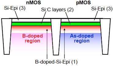
| Steep channel profile for 20nm-generation bulk CMOS. (1) A boron-doped Si:C layer is formed in advance of the Si:C interlayer formation. For the pMOS device, arsenic is used to dope the channel. (2) An Si:C interlayer is formed for both the nMOS and pMOS devices. (3) Finally, a silicon layer is formed on the channel surface by epitaxial growth, for both the nMOS and pMOS devices. (Source: Toshiba) |
Their new solution, "a simple process that adds a few layer-forming steps," forms three layers on the surface of the channel: a top layer of epitaxial silicon that functions as a low resistance path for electrons and holes; an intermediate layer of carbon-doped silicon (Si:C) to block impurity diffusion; and a boron-doped Si:C bottom layer to suppress the fixed charge accumulation in the gate insulator, caused by the Si:C layer formation. (For pMOS, arsenic was used to dope the channel.)
The results of this new structure are a 15%-18% performance boost vs. conventional channel structures; the new structure also can be applied to both nMOS and pMOS transistors to configure CMOS devices.
Spintronics-based MOSFET cell
Also at this week’s IEDM, Toshiba has disclosed what it claims is the first development and fabrication of a MOSFET cell based on spintronics with verified stable performance.
Spintronics — utilizing electrons’ spin and magnetic moment — is viewed as a potential replacement once MOSFET devices succumb to problems such as performance degradations (due to increased resistance in wiring) and power consumption (due to current leakage). The up/down spin states of electrons are more or less permanent in a magnetic layer, they note — i.e., a nonvolatile characteristic that can be used to store data; spin current flowing into the like spin state in a magnetic layer can change the impedance characteristics, which determines the read signal of a spintronics-based device.
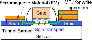
In its work, Toshiba introduced magnetic layers (formed with full-Heusler alloy, an intermetallic acting as a high spin polarizer) into the source/drain of a MOSFET cell, and applied them to controlling spin direction by a "spin-transfer-torque-switching" (STS) method and applying gate and S/D voltages. A magnetic tunnel junction (two layers of magnetic metals separated by an insulator to control resistance) is applied for write operation of the STS in the magnetic layers.
Tests indicate "the practical performance in transistor level" of such a spintronics-based device, promising fast random write/access speeds and low power consumption. Potential application is in next-generation nonvolatile semiconductor devices that can serve as reconfigurable logic devices, and nonvolatile LSI chips with memory function. Actual market introduction isn’t expected until at least 2015.
 |
| Diagram of Toshiba’s spintronics-based MOS field-effect transistor. (Source: Toshiba) |

