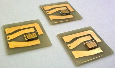
December 8, 2009 – At this week’s International Electron Devices Meeting (IEDM), IMEC has debuted a new GaN-on-Si double heterostructure field-effect transistor (FET) device offering low leakage and high breakdown voltage to help reduce power loss in high-power switching applications.
Traditional high-voltage power devices, based on Si-MOSFET structures, have generally reached intrinsic material limits; for a number of applications, their replacements are seen to be GaN compounds with high bandgaps (transport properties) and electrical breakdown field. Cost of GaN power devices is high, though growing GaN on large-diameter (up to 200mm) wafers can help keep costs lower vs. other substrates, IMEC notes.
In its work, IMEC says it has created a SiN/AlGaN/GaN/AlGaN double heterostructure FET structure on a Si substrate, based on an optimized process for selectively removing in-situ SiN. The resulting device achieved 980V high-breakdown voltage, with "excellent uniformity" and a low dynamic specific on-resistance of 3.5 mW.cm2. Combining that FET architecture with in-situ SiN grown in the same epitaxial sequence as the III-nitride layers resulted in e-mode device operation, something required for safety reasons, IMEC noted.
 |
| SiN/AlGaN/GaN field-effect transistor. (Source: IMEC) |

