December 14, 2009 – NEC Electronics disclosed two areas of work at the International Electron Devices Meeting (IEDM): a low-resistance copper interconnects with partially thickened local structure (PTL) to address resisitivity increases (and thus RF performance) in analog conductors, and high-threshold voltage-control gallium nitride (GaN) power transistors on a silicon substrate.
Low-resistance Cu interconnect
With CMOS scaling comes reduced sizes and spaces in which to fit interconnects, and the growing problem of increased parasitic resistance and capacitance, which degrades RF performance. Lowering gate-electrode interconnect as an input signal port in analog transistors can fix this. NEC says it has developed a low-k Cu dual-damascene contact interconnect technology, in which the insulating dielectrics are changed from silicon oxide (SiO2) to low-k dielectrics (SiOCH), and the contact metal alternated from high-resistive tungsten (W) to Cu. Burying Cu interconnect with Cu CT plugs in the low-k dielectric material over the CMOS transistor only improved RF performance by 10%, as gate-electrode interconnect resistance could not be reduced sufficiently.
Thus the team developed the new PTL, in which new Cu interconnects were formed (without any change in in-plain scaling) by selectively thickening specific parts of the low-k Cu DD CT structure 3-dimensionally; the other area remained connected only with the Cu CT plugs with low parasitic capacitance. In other words, the mixed configuration involved applying Cu CT plugs to the logic device areas where reduced capacitance is needed, and the PTL interconnect to analog areas (e.g., gate electrodes) where reduced resistance is needed for flexible design layout. Adding full low-k dielectric materials to the new PTL technology helps reduce parasitic capacitance as well as achieve low resistance, NEC noted.
Implementing the PTL-interconnect structure to connect the gate electrode as an input port of analog transistors for RF signals, NEC says it reduced input resistance of the Cu interconnect by 50%; RF performance was thus improved 30% to maximum oscillation frequency of >200GHz in the low-power 40nm node CMOS LSIs.
NEC also says that the "low-cost" fabrication process suppresses "microloading" in the RIE step (i.e., fluctuations in etch time/rate for opening patterns into dielectrics), by adopting both the new slit-shaped PTL interconnect as well as columnar-shaped Cu contact plugs required to connect CMOS transistors and Cu interconnects.
GaN power transistor on Si
NEC’s other announced work (in collaboration with parent organization NEC Corp.) was in the area of a nitride semiconductor power transistor on a silicon substrate with improved control and suppression of electrical currents when powered off. The device features a new structure for the layer beneath the gate electrode that improves controllability of threshold voltage that intercepts electrical currents, to enable low-power losses, high-speed switching, and high-temperature operations.
Nitride semiconductors promise lower-level losses, higher speeds, and higher temperature operations vs. conventional silicon transistors, but face the problem of variations of threshold voltage and reproducibility of normally-off characteristics. Current transistors use a two-layer structure (AlGaN electron supply layer and GaN channel layer), but threshold voltage variance occurs due to the AlGaN layer’s thickness beneath the gate, etched down from 20-30nm to a few nm to achieve normally-off characteristics. A high-precision etching process is needed to reduce those variations and stabilize those characteristics.
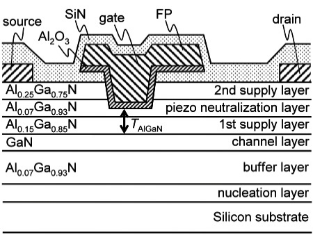
A five-layer structure, NEC proposes, would help transistors control threshold voltage by reducing dependence on that electron supply layer thickness — specifically, an electric charge neutralization layer ("piezo" neutralization layer) added to the electron supply layer, and a buffer layer under the channel layer with the same composition as the piezo one.
The structure enables "uniform manufacturing of nitride semiconductor power transistors that realize normally-off characteristics at a low cost," NEC claims in a statement. It plans to push ahead with R&D toward design, evaluation, and implementation of such nitride semiconductor power transistors.
 |
| Schematic cross-sectional view of the developed normally-off GaN MISFET with a piezo neutralization (PNT) structure. (Source: NEC) |

