by Pete Singer, editor-in-chief, Solid State Technology
December 8, 2009 – Scaling will continue at the traditional pace as defined by Moore’s Law well into the future. That was the conclusion by Ghavam Shahidi, IBM Fellow and director of silicon technology in IBM’s Research Division at Yorktown Heights, NY, who presented at the International Electron Devices Meeting (IEDM) during Sunday’s short course session. He predicted that — assuming EUV lithography becomes a viable option (which TSMC’s Burn Lin said was highly questionable, in a later presentation) — the industry would continue to rely on silicon to the 11nm node and beyond, although there would be a disruption in device architecture in the form of fully depleted (FD) devices. Companies are just now ramping 32nm devices into volume production and the industry is on track to move to the 22nm node in 2011. That will be followed by 15nm in the 2014-15 timeframe and the 11nm node in 2017-18. Further scaling to 8 and 5nm nodes will occur beyond 2020, perhaps enabled by silicon nanowires, Shahidi said.
There are many challenges in achieving this continued scaling, beyond those of lithography. Shahidi said increased substrate doping was one possible approach to reduce the device footprint in that it would allow a reduce depletion width under the gate. The concerns with this approach are that it could increase junction capacitance, cause gate induced drain leakage (GIDL), and create a challenge in getting to a low threshold voltage (Vt). Along with scaling the depletion width, researchers are also looking at scaling the junction depth to be equivalent to the inversion layer thickness, which would eliminate short channel effects (SCE). Shahidi said that if source/drain junction depths are less that the depletion layer width, then drain-induced barrier lowering (DIBL) is proportional to junction depth. However, there could also be an increase in source/drain resistance.
The advantage of fully depleted devices (FD) is an improvement in SCE. Extremely thin SOI (ETSOI) is one type of FD device. For a 22nm technology, the thickness of the FD layer needs to be less than 6-7nm. Another common FD device is the FinFET; here, fin thickness needs to be less than 15nm. The challenges with FinFET are that it’s difficult to obtain good profile control along a vertical wall (especially at a tight pitch) and there’s plenty of opportunity for excess parasitic capacitances. "Capacitances are intrinsic to the FinFET and they are significant," Shahidi said. "They can cause 10% or more performance degradation. You can get around it by decreasing pitch and increasing fin height, but you can see the challenge: we want to bring the fins closer and make them as tall as we can."
 |
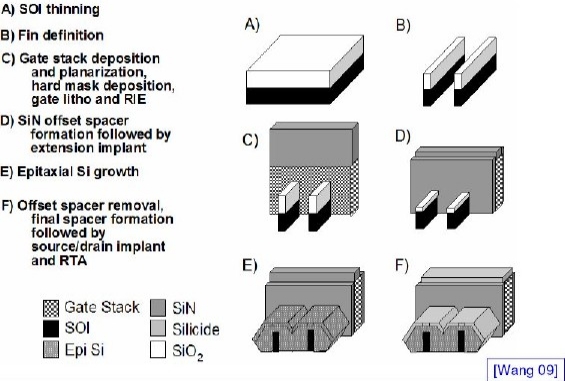
| Generalized FinFET process flow. (Source: IEDM/G. Shahidi) |
Fundamental challenges are profile control and etching of the spacers. "This is very difficult, especially in tight pitches," Shahidi said. "Gate profile control is a challenge."
A tri-gate approach is an interesting alternative to the FinFET, providing better SCE and comparatively very simple to implement. The tradeoff is that the tri-gate is not as tall and not as narrow. "As you form the spacer you’re really going to beat up on the top surface," Shahidi said.
Shahidi noted, however, that researchers have been able to achieve functional transistors with fairly small gate lengths using fairly traditional technology, including polysilicon/SiON gate stacks (vs. high-k/metal gates). Toshiba, for example, has presented a 14nm gate length device and Intel a 10nm device. Sub-10nm planar bulk devices have also been fabricated with a SiON gate dielectric and fully silicided (FUSI) gate, although raised source/drains were required.
The good news: even though challenges remain, Shahidi said that scaling has reduced variability. In terms of employing III-V materials in the channel region to increase mobility, he said he doubts if we’ll see that even at the 11nm node, "but we’ll see."
 |
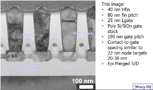
| Gate cross-section (TEM) of a FinFET with merged source/drain. (Source: IEDM/G. Shahidi) |

