by Hui-Jung Wu, Wen Wu, Roey Shaviv, Mandy Sriram, Anshu Pradhan, Kie Jin Park, Jennifer O’Loughlin, Kaushik Chattopadhyay, Tom Mountsier, Girish Dixit, Novellus Systems Inc.
EXECUTIVE OVERVIEW
Electromigration (EM) reliability has become a growing concern for Cu interconnects in advanced technology nodes. The interface between the dielectric diffusion barrier (SiCN) and copper, metal barrier quality and metallization homogeneity are all critical to EM performance. Our EM enhancement investigation has focused on improving the SiCN/Cu interface, metal barrier quality and metallization homogeneity while mitigating the process integration risk and cost. Multiple processes developed at Novellus have demonstrated significant EM improvement without compromising stress migration or dielectric reliability. The results of these process developments and the mechanisms of EM improvement will be discussed in this paper.
January 4, 2009 – Cu interconnect is now widely used in both logic and memory devices. With interconnect dimensions rapidly shrinking, following Moore’s law, meeting reliability requirements becomes more challenging. Numerous approaches, ranging from evolutional process optimization to novel process/materials adoption, are being explored to improve EM lifetime. Among these, dielectric diffusion barrier (SiCN) and metal barrier/seed processes have been the main focus. Enhancing the SiCN/Cu interface through plasma pretreatment and optimizing the key SiCN film properties have been widely adopted [1]. Metal barrier process optimization focusing on barrier step coverage, with re-sputtering, anchoring depth and via clean, have been reported previously [2-4]. Innovative approaches have also been proposed to improve EM through the adoption of novel materials/processes. Selective metal cap (CoWP) improves EM through the replacement of the critical SiCN/Cu interface with a strong metal-to-metal interface [5]. Other novel approaches such as Ru/Ti metal barrier [6], self-formed MnOx barrier [7], Ti metal barrier [8], and Ta implantation have also been reported [9].
Our investigation focused on the improvement of the SiCN/Cu interface, the metal barrier and metallization homogeneity. Integration results for PECVD Self Aligned Barrier (PSAB), HCM IONX Ta(N)/Cu process, HCM IONX Ti(N) metal barrier, new HCM Cu-Al alloy seed and PSAB/Cu-Al alloy seed synergies will be reviewed in this paper.
Experimental
A two-metal layer damascene structure with 65nm technology node features was used for the process integration study. HMS CORAL, a dense low-k (k=3.0) SiOC film, was used as the inter-line dielectric. The barrier layer was deposited in a Novellus INOVA system using HCM IONX Ti and HCM IONX Ta technology, respectively. Cu seed and Cu-Al seed were deposited in an INOVA system using HCM IONX Cu technology. The PSAB process was conducted on a Vector Multi-Station Sequential Deposition (MSSD) platform. A via-fed electromigration test structure, with nominal line dimensions of 100nm×180nm×500μm, was used for package EM testing. Via dimensions in the experiment are 90nm, with nominal aspect ratio of 2:1, and current density range and measurement temperature are 1.5-3MA/cm2 and 275-325°C, respectively.
Results and discussion
Metal barrier and seed optimization. The metal microstructure and the interface along the liner and cap layer are both critical to interconnect reliability [10]. Vias with high aspect ratios or "reentrant" profiles may lead to poor metal barrier coverage and the premature failure of the interconnect. Degradation of EM was observed when a non-uniform metal barrier process was used [3]. A barrier-first approach with re-sputter was developed to provide good step coverage for the via bottom corner and the "reentrant" area of the feature [2].
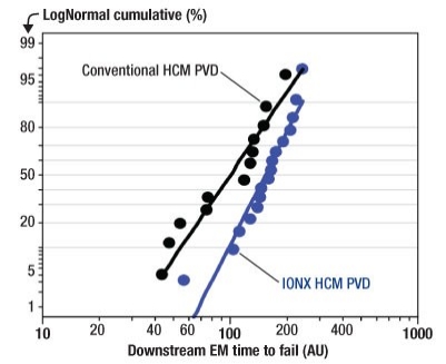
Additionally, with thinner barriers film morphology and density become increasingly important to maintaining barrier integrity and ensuring a good interface with the copper seed. HCM IONX Ta(N) uses a high density plasma and optimal ion energy with Hollow Cathode Magnetron (HCM) PVD technology to optimize the metal barrier microstructure. A high density metal barrier with smooth morphology and improved dielectric reliability was demonstrated in the experiment [11, 12]. Conformal copper seed step coverage is also essential to provide homogeneous metallization for the small features. RF copper deposition with resputter technology developed on the INOVA HCM source produces near-conformal copper step coverage. A combination of the HCM IONX Ta(N) and RF copper source leads to substantial improvements in Cu gapfill capability and EM performance. Significant improvements in both time-to-failure and sigma of distribution (Figure 1) are observed with the high density barrier and RF copper seed process [13].
 |
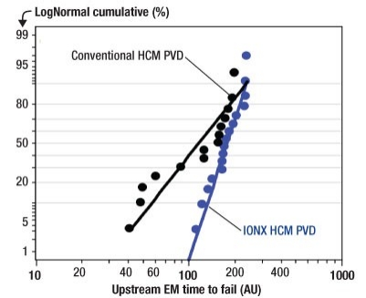 |
| Figure 1. Effect of barrier/seed on EM. Significant improvement in both TTF and distribution is observed with the IONX PVD relative to conventional HCM PVD. |
PECVD self-aligned barrier. The interface between SiCN and copper has been shown to be the main path for copper diffusion, and the weakest link in resisting EM failure. Many approaches have been explored to improve this SiCN/copper interface. Selective metal caps, such as CoWP, have demonstrated significant EM improvement and received much interest. The implementation of a selective metal CoWP cap, however, is expensive and difficult due to limitations in achieving good selectivity to deposition over copper versus dielectric surfaces, and may lead to degraded dielectric reliability. A self-aligned barrier, on the other hand, has good deposition selectivity and may be implemented through a slight modification to the SiCN unit process without degrading the electrical isolation characteristics of the intra/inter-metal dielectric layers.
The PECVD self-aligned barrier (PSAB) has attracted much attention recently due to its high selectivity, low cost of implementation and benefits to interconnect reliability [14, 15]. The typical process steps in forming a PSAB have been described previously [16]. High selectivity of the PSAB process arises through the natural differences in reactivity and reaction products of the gaseous constituents with the Cu and dielectric surfaces. In the case of Si-based PSAB, SiH4 exhibits thermally-activated reaction with Cu, but the reaction on the dielectric surface results in the formation of an insulating film. Similarly, Ge reacts rapidly with Cu as shown in the SIMS analysis, but electrical testing shows no indication of Ge reaction with various dielectric films [16].
 |
| Figure 2. Downstream EM for the control and Ge-PSAB splits. Ge PSAB significantly enhances EM lifetime over control. |
Significant improvement in mean-time-to-failure (MTTF) for the downstream EM test is noted with the integrated Ge-PSAB scheme as compared to the control (Figure 2). Details of the mechanism for EM improvement are still under investigation. Previously, we reported TDDB and EM improvements associated with improved adhesion of the low-k SiC to both Cu and low-k dielectric, enabling better encapsulation of the Cu inside the trench [15]. In this work, adhesion energy measurements for both the control and Ge-PSAB/Cu interfaces were measured to be high and similar. The distribution of the Ge inside the Cu shows a higher concentration of Ge near the Cu-SiCN interface [16]. The thin layers of CuGex may aid in retarding the growth of the nascent defects (voids) within the interconnect structure. In addition, the cladding layers around the Cu surface create a shunt layer around the lower resistivity conducting metal, diverting the current away from the weaker interface. Diffusion of Cu with the electron wind would disturb the metallurgical equilibrium of the CuGex/Cu structure due to increases in the concentration of Ge in Cu-depleted areas near the interface. This creates a net force proportional to the concentration gradient, opposing electromigration [16]. The above-mentioned mechanisms would lead to void growth delay without changing the failure mode. This is consistent with our investigation, where the EM activation energy of the Ge-PSAB is similar to that of reference SiCN, but the EM time-to-failure is much longer.
Alloy seed. Metal alloying has been widely used in semiconductor processes since the Al-interconnect era. Multiple Cu-alloying elements and approaches were investigated to improve reliability [17]. Cu-Al alloys have received much attention. It was observed that alloying Cu with Al increases the incubation time for void growth and decreases the Cu drift velocity [18]. PVD processing has been the preferred approach for Cu alloying due to the readily-available alloy targets, lower cost and easier process control. The alloying of Cu with Al, however, increases the Cu interconnect resistance and thus degrades RC delay. Our investigation of Cu-Al alloy seed integration focused on the tradeoff between increased resistance and improved reliability, with the goal of minimizing the RC delay degradation while maintaining the benefits of Cu-Al alloy seed. Through this process development and integration optimization, a new alloy seed process was developed.
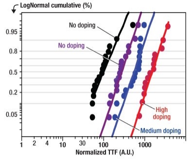 |
| Figure 3. Downstream EM TTF as a function of Al doping concentrations for samples with conventional alloy seed. |
The downstream package electromigration test results suggest clear correlation between time-to-failure (TTF) and Al doping concentration for conventional alloy seed process (Figure 3). Significant EM improvement can be achieved with the Cu-Al alloy approach, but it leads to a large increase in RC delay. A measure of the tradeoff between EM improvement and an increase in RC delay, defined as the "EM improvement efficiency", was recently proposed by S. Yokogawa et al. [19]. Here it was concluded that with conventional Cu-Al alloy seed — while significantly improving EM lifetime the EM improvement efficiency was not as high as with the CoWP metal cap approach.
A new alloy seed approach was developed with the HCM PVD process to enhance the EM improvement efficiency without compromising dielectric reliability and stress migration performance [11]. The EM improvement with alloy seed as a function of the normalized line resistance is plotted in Figure 4. Consistently higher EM improvement efficiency, defined as the slope of the plot in Fig. 4, is demonstrated with the new HCM alloy seed process. This process allows the use of a PVD process based on HCM technology to provide EM improvement for advanced technology nodes.
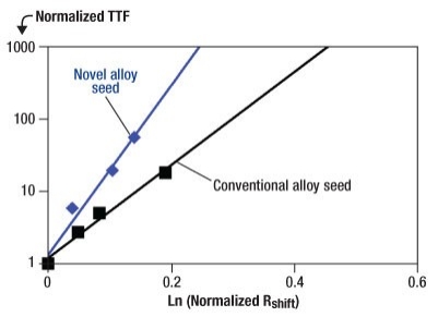 |
| Figure 4. Comparison of the "EM improvement efficiency" between new HCM and conventional alloy seed process. Consistent higher EM improvement efficiency is observed for new HCM alloy seed process. |
The improvement in EM with a Cu-Al alloy is attributed to a slower Cu drift velocity and a lower void growth rate [19]. SIMS depth profile analysis indicates Al diffuses through Cu and accumulates at the SiCN/Cu interface upon thermal anneal [12]. It is hypothesized that the Al getters the residual oxygen at the SiCN/Cu interface, driving the segregation at the SiCN/Cu interface and improving electromigration. The improvement of the SiCN/Cu interface, along with slower Cu drift and reduced Cu void growth rate, greatly enhances electromigration performance with use of the Cu-Al seed. While the mechanisms are still under investigation, we believe that this new HCM alloy seed process allows the formation of a homogeneous Cu microstructure inside small features and strengthens the Cu/SiCN interface, leading to improved EM resistance.
Ti(N) metal barrier. The need for reliability improvement also led us to investigate alternative metallization approaches. A Ti(N) metal barrier was once considered to be inappropriate for Cu metallization due to potential F attack from fluorine-doped silicate (FSG). However, as carbon-doped oxide (CDO) replaces FSG for interconnect dielectrics, interest in Ti(N) barrier as the metal barrier has returned.
The interfaces between the Cu/Ti(N) metal barrier, Ti(N)/dielectric and SiCN/Cu are all critical to the reliability performance. Our dewetting investigation result suggests poor Cu wetting behavior on TiN, but excellent Cu wetting on Ti. However, Ti is known to diffuse into Cu, raising Cu resistivity, and is not able to provide the needed barrier properties. Here, a composite Ti/Ti(N)/Ti layer is proposed to address both Cu/Ti(N) interface and Cu diffusion barrier concerns [20].
No RC delay is observed with an optimal Ti(N) process, even though Ti diffusion into Cu is detected. This result can be attributed to accelerated Cu grain growth when Ti(N) is used as the metal barrier. Larger Cu grain alleviates the Cu resistivity increase due to Ti doping. SIMS profile analysis indicates Ti aggregation at the SiCN/Cu interface, similar to our observation with Cu-Al alloy seed. Ti also acts as an oxygen getter at the interface, and reinforces the SiCN/Cu interface. This mechanism is further supported by the higher adhesion energy and detection of TiOx at the SiCN/Cu interface. Significant EM improvement is observed with a Ti(N) metal barrier, as shown in Figure 5.
 |
| Figure 5. Downstream EM performance for Ta(N) and Ti(N) based metal barrier. 10× longer EM TTF is demonstrated with Ti(N) based metal barrier. |
Process synergy. Multiple paths were explored for improvement of EM. A PSAB approach enhances the SiCN/Cu interface with the formation of a shunt layer near the SiCN/Cu interface, prolonging the voids growth within the interconnect structure. An alloy seed approach improves the EM performance through different mechanisms. The capability to combine various low cost, low risk reliability improvement approaches to meet the increasing reliability challenges provides greater benefits than employing radical process changes.
Figure 6 illustrates our preliminary result in exploring the synergistic effect of combining PSAB and alloy seed processes. The result shows improvement, whether with PSAB or Cu-Al alloy seed alone. Combining PSAB and Cu-Al seed leads to further improvement in EM time-to-failure. This synergy is not limited to PSAB and alloy seed, but is also applicable to other approaches. Recent studies suggest a similar synergy between the self-aligned barrier and the MnO barrier [21].
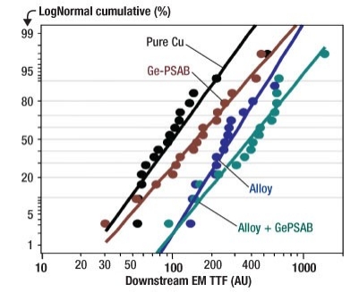 |
| Figure 6. Progressive improvement in EM is demonstrated with Ge-PSAB, alloy seed, and Ge-PSAB + alloy seed. |
Conclusion
We have demonstrated multiple paths to improve EM performance. Optimization of the metal barrier and copper seed processes provides reliability improvement through a high quality metal barrier and homogeneous copper metallization. Further EM enhancement can be achieved through a novel copper alloy seed approach, which provides higher EM Improvement Efficiency over conventional Cu-Al alloy seed. The PSAB process shows significant EM improvement without compromising dielectric reliability. Furthermore, synergy between the Cu-Al alloy seed and PSAB demonstrates the capability to combine these different approaches to maximize the electromigration benefit. Finally, a significant EM improvement was observed with Ti(N) metal barrier integration, and RC delay was not compromised with the use of the Ti(N) metal barrier.
Biography
Hui-Jung Wu is senior technologist at Novellus Systems Inc., 4000 North First St., San Jose, CA 95134 USA; ph.: (408) 570-2978; e-mail: [email protected].
Acknowledgments
Wu, H.-J., Wu, W., Shaviv, R., Sriram, M., Pradhan, A., Park, K. J., O’Loughlin, J., Chattopadhyay, K., Mountsier, T., and Dixit, G., "Electromigration Improvement for Advanced Technology Nodes," ECS Transactions, Vol. 18, No. 1, p. 269 (2009). Copyright © The Electrochemical Society.
This paper was first published at China Semiconductor Technology International Conference (CSTIC) 2009.
PSAB is a trademark of Novellus Systems Inc.
IONX, Coral, INOVA, Vector, and HCM are registered trademarks of Novellus Systems Inc.
References
[1]. Y. Zhou, et al., "Impact of Interfacial Chemistry on Adhesion and Electromigration in Cu Interconnects," Proc. of the AMC, p. 189, 2004.
[2]. G.B. Alers, et al., "Barrier-First Integration for Improved Reliability in Copper Dual Damascene Interconnects," Proc. of the IITC, p. 27, 2003.
[3]. K.-D. Lee, et al., "Via Processing Effects on Electromigration in 65nm Technology," Proc. of the IRPS, p. 103, 2006.
[4]. A.H. Fisher, et al., "Reliability Challenges in Copper Metallizations Arising with the PVD Resputter Liner Engineering for 65nm and Beyond," Proc. of the IRPS, p. 511, 2007.
[5]. S. Gall, et al., "Investigation of the Impact of CoWP Self-Aligned Barrier Deposition on the Porous SiOC Properties after a Direct CMP Process," Proc. of the IITC, p.126, 2008.
[6]. M. Tagami, et al., "Highly-Reliable Low-Resistance Cu Interconnects with PVD-Ru/Ti Barrier Metal toward Automotive LSIs,", Proc. of the IITC, p. 205, 2008.
[7]. T. Watanabe, et al., "Robust BEOL Process Integration with Ultralow-k (k=2.0) Dielectric and Self-Formed MnOx Barrier Technology for 32nm-Node and Beyond," Proc of the IITC, p. 208, 2008.
[8]. A. Sakata, et al., "Reliability Improvement by Adopting Ti-barrier Metal for Porous Low-k ILD Structure," Proc. of the IITC, p. 101, 2006.
[9]. J. Gambino, et al., "Reliability of Cu Interconnects with Ta Implant," Proc of the IITC, p. 22, 2007.
[10]. A.H. Fisher, et al., "Process Optimization-The Key to Obtain Highly Reliable Cu Interconnects," Proc of the IITC, p. 253, 2003.
[11]. H.-J. Wu, et al., "Improving Interconnect Reliability via Optimized Barrier/Seed," Semiconductor International, No. 11, p. 38, 2008,
[12]. S.B. Law, et al., "Impact of Barrier Film Characteristics on Vramp Breakdown Voltage & TDDB Lifetime of 65nm Node Cu/Low-k Interconnects," Proc. of the AMC, p. 133, 2007.
[13]. R. Shaviv, et al., "Improvements in Electromigration to Meet the Requirements of Advanced Technology," Proc. of the AMC, p. 81, 2008.
[14]. K. Chattopadhyay, et al., "In situ Formation of a Copper Silicide Cap for TDDB and Electromigration Improvement," Proc. of the IRPS, p. 128, 2006.
[15]. T. Usami, et al., "Highly Reliable Interface of Self-Aligned CuSiN Process with Low-k SiC Barrier Dielectric (k=3.5) for 65nm Node and Beyond," Proc of the IITC, p. 125, 2006.
[16]. H.-J. Wu, et al., "Self-Aligned Barrier Improves Interconnect Reliability," Semiconductor International, No. 5, p. 34, 2008.
[17]. K. Barmak, et al., "On the Use of Alloying Elements for Cu Interconnect Applications," J. Vac. Sci. Technol. B, Vol. 24, No. 6, p. 2485 (2006).
[18]. S. Yokogawa et al., "Effect of Al Doping on the Electromigration Performance of Damascene Cu Interconnects," J. Appl. Phys., Vol. 101, p.013513 (2007).
[19]. S. Yokogawa, et al., "Tradeoff Characteristics Between Resistivity and Reliability for Scaled-Down Cu-Based Interconnects," IEEE Trans. on Elec. Dev., vol. 55, No. 1, p. 350 (2008).
[20]. W. Wu, et al., "Ti-based Barrier for Cu Interconnect Applications," Proc. of the IITC, p. 202, 2008.
[21]. H. Kudo, et al., "Further Enhancement of Electro-Migration Resistance by Combination of Self-Aligned Barrier and Copper Wiring Encapsulation Techniques for 32nm Node and Beyond," Proc. of the IITC, p.117, 2008.

