by C.L. Hsueh, A. Bavin, Aviza Technology; J. Monkowski, C. Borowski, Pivotal Systems Corp.
Executive overview
With semiconductor technology continuing to follow Moore’s law at a seemingly increasing pace, it is ever more critical for chipmakers to find new ways to increase productivity and reduce cost. Additionally, new materials are providing challenges to existing process chamber conditions and process chamber characterization. The ability to clean process chambers in situ can provide improvements in tool availability as well as reduce consumable parts wear and cost.
January 11, 2009 – Integration of high-k gate dielectrics in sub-45nm CMOS devices requires the gate electrode material to be changed from polysilicon to metal. Polysilicon electrodes are unsuitable as the material can react and diffuse into the high-k gate dielectric, leading to the formation of a silicide that reduces the overall k value of the gate stack. In addition, the relatively low concentration of electrons in the polysilicon leads to rapid depletion and causes a significant increase of the gate EOT.
The choice of the electrode metal is largely defined by the ease of integration, cost of deposition and effective work function (eWF) required from the gate stack. Although the eWF can be adjusted by changing the internal potential of the gate dielectric through addition of a dipole layer, selection of the correct metal for the electrode can have a significant effect as shown in the table below.
| Device type | NMOS | PMOS |
| ITRS work function target | <4.25eV | >4.95eV |
| Reported polysilicon results | 4.05eV | 5.15eV |
| Reported metal results | TaCx = 4.2 to 4.5eV TaTbxN = 4.23eV |
Ru=5.03eV |
Several techniques have been used to deposit metal electrodes, though atomic layer deposition (ALD) most closely meets the application requirements. In a manufacturing environment, the process repeatability offered by ALD enables high process yields and reduces production costs. However, compared with competing deposition technologies it has a relatively low process throughput, so module uptime becomes key to achieving acceptable productivity. Aviza developed a two-step in-situ plasma cleaning process that improves the uptime of ALD process chambers by reducing the mean-time-to-clean (MTTC) and increasing the mean-time-between-clean (MTBC).
The plasma clean process was performed using plasma activation of nitrogen trifluoride (NF3). The plasma was generated from a pulsed UHF power supply connected to the wafer stage. A Sensor X provided by Pivotal Systems was used to monitor the chamber ambient for purposes of end point detection and residual gas analysis. The connection point was chosen to minimize intrusion into the process chamber and restriction of maintenance access.
The monitor is a small plasma-based sensor that produces atomic-level insight into the process chemistry. Process gases diffuse into the sensor’s inner cavity where they are excited by a high-density plasma that breaks down the molecules into their atomic elements. This allows the user to easily interpret discrete spectral species. It attaches directly to the process chamber via standard vacuum fittings. The sensor system consists of a 13.56MHz RF supply and uses standard OES (optical emission spectroscopy) to analyze the atomic emissions. A computer server collects and analyzes the spectral data in real-time for end point applications.
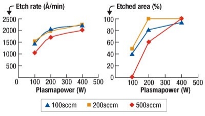
A matrix of process tests was performed to evaluate the effect of NF3 flow and plasma power. Very high etch rates in excess of 2000Å/min were achieved for NF3 flows of 100, 200, and 500sccm at the maximum power of 400Watts. However, the etching was seen to be non-uniform across the process chamber as shown in Figure 1. A uniform etch process with an etch rate of 1900Å/min was achieved with an NF3 flow of 200sccm and a plasma power of 200W.
 |
| Figure 1. Optimization of etch rate and uniformity through NF3 flow and UHF plasma power. |
Using these conditions, the process chamber could be effectively cleaned in the region above the wafer stage, but deposition was still evident below the stage. Though this would not be an issue for other processes, the ALD process uses sequential pulse and purge of process gasses which could disturb loose material from below the stage and transport it onto the wafer surface. Therefore, a two-step process was developed to clean the top and the bottom of the process chamber independently. By changing the vertical position of the stage it was possible to strike the plasma behind the stage leading to uniform cleaning of the lower part of the chamber. Coupon tests showed that this process has a selectivity of >15,000:1, indicating that damage to the process chamber would be minimal.
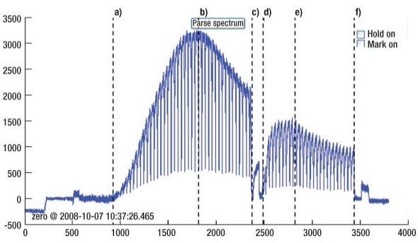
Results from the monitor clearly showed that a process end-point can be seen from both parts of the two-step etch process. For this test, the sensor was monitoring the chamber for a Ti emission at 498nm. The fluctuations in the Ti signal are caused by the pulsing of the UHF plasma power. An important consideration in the placement of the Sensor X is that there should be very little delay between the condition in the chamber near the wafer environment and the reading from the sensor. The sharp transitions in the signal shown in Figure 2 as the UHF plasma turns on and off indicate that the signal from the sensor is in fact very representative of the wafer environment, with very little delay. Therefore, we can assume that the process end-point occurs at the point where the Ti signal starts to drop. For the purposes of this test, a timed etch process was run to remove 1.5μm of deposited TiN from the chamber. By controlling the etch process from the sensors end-point signal it would be possible to minimize the over-etch time and achieve at total etch time of 18.3min, which is equivalent to an overall etch rate of 819Å/min.
 |
| Figure 2. Sensor X output showing Ti emission during 2-step plasma cleaning of TiN. The following aspects of the process can be observed: a. Step 1 process start, b. Step 1 process end-point, c. Step 1 process end, d. Step 2 process start, e. Step 2 process end-point, f. Step 2 process end. |
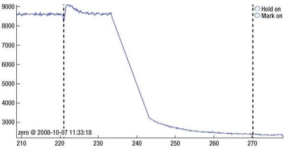
After etching, the Sensor X was used to monitor the residual gas remaining in the process chamber and, as expected, a significant level of fluorine (F) remained. The F must be removed from the chamber prior to further processing as it will be incorporated into the deposited metal electrode leading to process instability. By employing a simple H2 plasma after the cleaning process the F could be rapidly removed as shown by the emission signal in Figure 3.
 |
| Figure 3. Sensor X output showing F emission during H2 plasma following cleaning of TiN. Only residual traces of F are detected after 35s. |
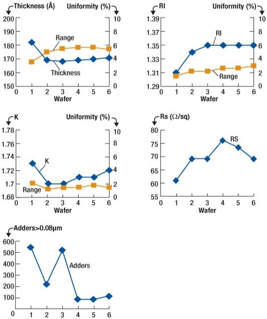
To confirm the performance of the ALD process after the etch and F removal processes, six TiN test films of 150Å thickness were deposited sequentially and measured for film thickness, refractive index, coefficient of extinction, sheet resistance and particle adders. TiN was chosen for this test as it is known to be sensitive to chamber contamination. The results obtained show that the chamber is effectively conditioned after 600Å of TiN deposition indicating that all remaining F has been eliminated from the process chamber.
Conclusion
The two-step plasma cleaning process was proven to be a fast and effective method of maintaining a high uptime and high productivity for ALD of Ti and Ta based electrode materials. The high etch rate, in situ measurement capability, rapid F removal, and short process conditioning time enabled an 80% reduction in MTTC and an estimated 10× increase in MTBC. The process has a high selectivity to the material of the process chamber and internal shielding suggesting that chamber components may be reused to further reduce the process cost.
 |
| Figure 4. Results from the TiN process conditioning tests performed immediately after the chamber clean process. All results appear normal by wafer number 4. |
Acknowledgment
Sensor X is a trademark of Pivotal Systems Corp.
Biographies
C. L. Hsueh is at Aviza Technology, 440 Kings Village Rd., Scotts Valley, CA 95066 USA.
Andy Bavin received his BS in physics from the U. of Bath, England and is a product manager at Aviza Technology.
Joseph Monkowski received his BS, MS and PhD in electrical engineering, and an MS in materials science, all from Penn State U. He is president and CTO at Pivotal Systems Corp., 4683 Chabot Drive, Pleasanton, CA 94588, USA.
C. Borowski received his BS in general engineering from the U.S. Naval Academy and an MBA in management from Golden Gate U. He is a senior product manager at Pivotal Systems Corp.
References
[1]. K. Choi et al., "Growth mechanism of TiN film on dielectric films and the effects on the work function," Thin Solid Films 486, pp. 141-144, 2005.

