by James Word and Xima Zhang, Mentor Graphics
Executive overview
The remarkable progress of Moore’s Law in doubling the transistors per chip every two years has been enabled by the rapid advances in microlithography, such as smaller wavelength, larger numerical aperture (NA), and off-axis illumination. However, because of the limitations of 193nm lithography, much of the shrink capability is now coming from the computational lithography domain, where software-driven advancements in optical proximity correction (OPC) and resolution enhancement technology (RET) allow for printed features far below the diffraction-limited resolution of the exposure equipment. This article discusses solutions for the computational load challenges that arise from the increasing complexity of the industry’s lithography roadmap.
January 12, 2010 – The growth of computational lithography — including sub-resolution assist features, phase shifting masks, double patterning or double exposure — comes with its own challenges. Perhaps the most significant consequence is the tremendous amount of additional computation required. The increases in computational load are driven by three factors: increasing layout density, tighter critical dimension (CD) budgets, and the end of scaling from lithography tools. These three factors mean that any given design below the 32nm node has more to simulate, requires higher model accuracy, and involves computational scaling techniques. The costs of this growing computational load are seen in longer turn-around-times (TAT) that delay products, and the need for more CPUs and the energy to operate them [1].
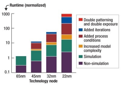
How serious is this growth in post-tapeout computational load? We estimate that if nothing is done to address the problem, the computational load required for OPC will jump 1000× between the 65nm and 22nm nodes (Figure 1). For example, assume that 200 CPUs are required for reasonable post-tapeout TAT on a 65nm design. Maintaining the same schedule at 22nm would require 200,000 CPUs. Factor in the additional hardware, software licenses, and infrastructure expenses, and the costs of keeping up with this post-tapeout trend quickly become untenable.
 |
| Figure 1. The historical and projected trend in OPC computational loads indicates a 1000× increase between the 65nm and 22nm nodes if nothing is done to ameliorate the burden. |
Solutions to OPC computational demands
This dramatic and unsustainable trend has led to new tools, flows, and methodologies for managing TAT and cost in the post-tapeout flow. The solutions include some combination of the following:
- Upgrade to faster standard (usually x86) hardware
- Dense simulation
- Software improvements
- Hardware specialization (i.e., co-processor acceleration)
More and better hardware plays a role in managing OPC computation loads. Fortunately, OPC lends itself to parallelization, hardware is relatively cheap, and it delivers steady performance improvements. Some of the newer CPUs have 2× more memory bandwidth, and handle multithreading significantly better than previous generations. However, even with hardware improvements, there are limits to the ability of distributed computing in controlling TAT. More standard hardware alone will not be enough to manage the additional computational loads. The solution also requires considerable software improvements and specialized hardware acceleration.
The most significant software improvement in the OPC domain has been the transition from ‘sparse’ to ‘dense’ simulation. Sparsely computed aerial image computation, where images are computed only where needed and in the spatial domain, was the most efficient method for computing images at the 65nm node and above. Sparse OPC simulation time depends on the number of sites per chip (which is driven by layout density), and the time to compute each site (which is driven by the models). This leads to an exponential increase in simulation time with shrinking process nodes.
Dense image computation, where the layout is partitioned into frames, and each frame across the chip is simulated in the frequency domain, has become the most efficient method at the 45nm node and below. The simulation time of dense OPC is dependent mostly on the number of fast Fourier transform (FFT) frames per chip, which is proportional to the Nyquist sampling distance. The processing time for each frame remains constant with each technology node, and there are only slightly more frames at each node, which leads to a linear growth in simulation time.
The optimum choice of sparse or dense simulation is often layer-dependent, so a given technology node will require a mixture of both simulation methods to achieve the minimum OPC runtime. High density layers, like metal 1 and poly, need to transition to dense OPC first. Via layers still do better with sparse OPC.
Accelerating dense simulation
The use of dense simulation in OPC software has the advantage of being very amenable to hardware acceleration. Dense simulations are composed of FFTs and other operations that can be accelerated on specialized hardware such as the Cell Broadband Engine. Co-processor acceleration is easy to add on to existing compute clusters, is expandable, and is more flexible in production tape out environments than dedicated OPC-only compute architectures. Dense simulations with hardware acceleration can be up to 30× faster than those performed on conventional x86 processors.
In addition to more hardware, the use of co-processor acceleration, and improved simulation algorithms, other improvements in OPC/RET software play a key role in managing costs and TAT in the post-tapeout flow. For example, Mentor Graphics’ OPC software has improved performance by 3× in the last two years. This speedup is a result of optimizations to the core simulation algorithms and related software code [2].
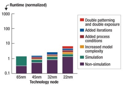
Using software optimization combined with hardware improvements, we have achieved runtimes on 22nm designs that are under 10× the runtimes for 65nm designs, despite the huge increase in simulations required (Figure 2). This TAT control was achieved using a combination of OPC simulation types, optimized OPC software, newer x86 processors and CBE co-processor acceleration.
 |
| Figure 2. With the right combination of simulation method, hardware, and software, OPC TAT at 22nm can be contained. The 65nm cases used all sparse simulation and x86 CPUs. Dense simulation was added for the 45nm cases. For the 32nm cases, we added newer x86 cores and co-processor acceleration. The 22nm cases also used the latest optimized OPC software. |
Conclusion
Assembling, configuring, and tuning the right combination of all the available computational lithography tools and techniques requires experience and expertise, but is well worth the effort. Mask engineers need to be actively engaged with their vendors in building solutions to manage runaway OPC runtimes. While migrations to the 32nm and 22nm nodes present significant challenges for maintaining TAT and cost control in the post-tapeout flow, a tailored and multi-prong solution can keep Moore’s law marching forward.
Biographies
James Word received his BSEE from the U. of New Mexico and is product manager for OPC at Mentor Graphics, 8005 SW Boeckman Rd., Wilsonville, OR 97070; ph.: 503-685-1172; e-mail [email protected]. He has over 15 years of experience in the semiconductor industry, in the areas of OPC and photolithography technology development.
Xima Zhang received his Ph.D in manufacturing engineering from Boston U. and is a technical marketing engineer at Mentor Graphics.
References
[1] C. Albertalli, T. Kingsley, "Computational Lithography Drives DFM Cost of Ownership," Semiconductor International, May 5th, 2007.
[2] A. Nouh, M. Park, "Compute Resource Management and TAT Control in Mask Data Preparation," Proc. SPIE Vol. 7272, February 2009.

