February 2, 2010 – The move to the 2Xnm NAND flash node gives Intel and Micron a big step ahead of competitors in terms of cost and pricing, an advantage they will likely ride out as profit instead of squeezing prices further, according to an analyst.
The details
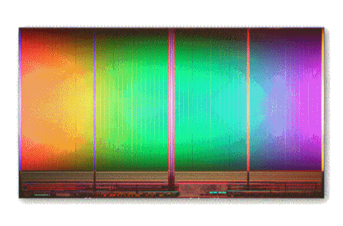
The new 167mm2 NAND chip, built with 25nm process technology — "not only …the smallest NAND technology, [but] also the smallest semiconductor technology in the world," the companies’ JV, IM Flash, points out in a statement — presses 8GB of storage into a single device, >10× the data capacity of a standard CD. The device offers the highest density in a 2 bits/cell multilevel cell die, that can fit in a standard thin small-outline package (TSOP), and multiple such devices can be stacked in a package — a 256GB solid-state drive could be built with just 32 such devices (half as many as before), a 32GB smartphone would need just four, and a 16GB flash card requiring only two. The 25nm 8GB device is now sampling, with mass production slated for 2Q10.
 |
| Intel/Micron’s 25nm 8GB NAND flash memory device. (Source: Intel) |
Analyst’s take
Jim Handy from Objective Analysis does the math on the new chip: The size of the device suggests about 400 dice can be built on a (300mm) wafer, which he calculates at about $4.00/chip, or $0.50/GB. That’s less than a third of the cost/GB of a typical 45nm MLC NAND on a 300mm line (about $1.75/GB), he notes. NAND flash prices have been "hovering at around $2.00/GB for the past year," and Intel/Micron’s 34nm chip costs about half that ($1.00/GB) — so either Intel/Micron could just pass along those big cost savings at 25nm and squeeze rivals, or it can just sit tight and pile up the profits. Intel and Micron clearly state they want to do the latter.
Handy also notes that migrating to the new 25nm process not only helps build a profit war chest vs. rivals, but it helps them "squeeze more gigabyte production out of their Lehi and Manassas lines before having to equip their new fab in Singapore," he writes.
In the video below, Brian Shirley, VP of Micron’s memory group, talks more about the 25nm NAND flash device, and progress on other tech boundaries such as multibit/cell (>2bit) architectures, charge-trap, and vertical scaling.

