|
Executive OVERVIEW A comparative study of the advanced boron-based ultra-low energy doping techniques on USJ fabrications, including beam-line atomic 11B implant; BF2, B18H22, C2B10H12 molecular implants, cluster B implant, and B2H6 and BF3 plasma doping implants is presented in this paper. Recently, much has been published about USJ fabrications where different advanced ULE doping techniques combined with different PAI and co-implants and advanced annealing techniques were used. The results are sometimes contradictory and confusing because of the lack of valid comparisons and metrology limits. The work presented here is an attempt to provide clarity. |
Shu Qin, Y. Jeff Hu, Allen McTeer, Micron Technology, Inc., Boise, ID USA
The focus of this paper is a comparative study of the advanced boron-based ultra-low energy doping techniques on USJ fabrications, including beam-line atomic 11B implant, BF2, B18H22, C2B10H12 molecular implants, cluster B implant, and B2H6 and BF3 PLAD implants. For a fair comparison, we did not employ PAI and co-implants and advanced anneals. A conventional lamp-based spike RTP is employed for activation and annealing.
ULE implants
To meet USJ roadmap requirements [1], ULE ion implants must be used. However, the conventional beam-line ion implants are encountering three major issues in the ultra-low energy implant regime. First, the space charge limit causes unacceptable throughput of low energy high dose implants. Second, the self-sputtering effect causes device modification and dopant and RS saturations. Third, implant angle variation causes difficulties for non-planar structures. There have been several alternative doping methods, such as molecular ion implants using BF2, B10H14 (decaborane), B18H22 (octadecaborane), C2B10H12 (carborane) ion species [2-4], and cluster B ions using hundreds to thousands of B atoms to form very large cluster ions [5,6], which have been developed to overcome the space charge limit and enhance the productivity of low energy high dose implants. Moreover, plasma doping (PLAD) or plasma immersion ion implantation (PIII) techniques using B2H6 (deborane) or BF3 (boron trifluoride) gas species have been developed to overcome all three of these major physical limits of the conventional beam-line ion implants [7-10]. PLAD is a doping technique that is a simpler system, has a lower cost, higher throughput, and device performance improvements [7-10].
Experiments
The starting materials are 300mm blanket <100>-oriented n-type single-crystalline wafers. The process conditions of the conventional beam-line ion implant include ion species 11B+; energy 500eV; dose 1×10¹⁵/cm2; with implant tilt angle 0°. The molecular beam-line ion implants of BF2, B18H22, C2B10H12 and cluster B used 11B+, 500eV energy, and 1×10¹⁵/cm2 dose equivalent conditions based on energy/mass ratios and RS-xj characteristics. For example, BF2 implant used 2500eV energy with 1×10¹⁵/cm2 B+ dose, and B18H22 implant used 10keV energy with 5.56×10¹³/cm2 B18H22+ dose (1×10¹⁵ B+ dose). The PLAD system is a continuous RF-excited pulsed plasma-doping system, described in detail elsewhere [10]. The PLAD process conditions are also 11B+, 500eV energy, and 1×10¹⁵ B+ dose equivalent conditions. For example, B2H6 PLAD used nominal -1.2kV voltage and 5×10¹⁵/cm2 total dose, and BF3 PLAD used nominal -1.7kV voltage and 4×10¹⁵/cm2 total dose. After implants, the wafers were cleaned by standard strip and clean processes to mimic the real production photoresist remove and clean processes. The annealed wafers were processed using a spike rapid thermal-annealing process (RTP) to activate the impurities with a condition of 1000ºC/spike in pure N2 ambient. The spike RTP anneal was performed on an Applied Materials Model Vantage RadiancePlus system. The spike RTP parameters include 550ºC kick-up temperature, ~130ºC/sec ramp-up rate, ~70ºC/sec ramp-down rate, and ~3.5 sec effective thermal budget at 1000ºC ±150ºC.
Several new metrologies are used to characterize the ULE doping process: SIMS/ARXPS [11] for impurting profiles and doses, ARXPS [12] for self-sputtering/etching/deposition effects, non-contact RsL [13] for shees resistance Rs and CAOT/DHE [14] for carrier dose and mobility.
Table 1 lists USJ implant experiment matrix and results. xj is defined at 5×10¹⁸/cm3 background concentration, and abruptness is defined by a depth when B concentration drops a decade from 1×10¹⁹ to 1×10¹⁸/cm3. The total B dose includes B in native oxide and Si. The retained B dose in Si is only B in Si substrate. Activated B dose is calculated from SIMS profiles by integrating B profiles under the boron solid solubility (BSS) level. BSS is ~1.8×10²⁰/cm3 at 1000ºC anneal temperature [15]. DHE RS is defined from CAOT/DHE data and calculated by
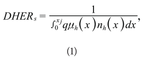
where q is electron charge, μh(x) is the hole drift mobility profile and nh(x) the carrier (hole) profile measured by CAOT/DHE, and xj is the junction depth.

Table 1 demonstrates that the native oxides play a very significant role on ultra-low energy implants and dominates the B impurity loss and B redistribution mechanisms [16]. B loss into the surface native oxides is more severe in the ultra-low energy regime. For beam-line implants, around 50% of the total implanted B doses are trapped and lost into the native oxides. Cluster B implant lost 2/3 of the total implanted B dose due to its non-Gaussian and more shallow profile. B2H6 and BF3 PLAD implants lost 2/3 and 4/5, respectively of the total implanted B doses due to PLAD’s unique exponential-like B profiles [8-10]. The B components in the native oxide must be extracted from the total B dose because the B dose in the oxide cannot be activated and will be lost by subsequent clean processes, such as pre-clean for metal contact deposition. The B loss into native oxides is a main mechanism of B loss for both as-implanted and annealed wafers.
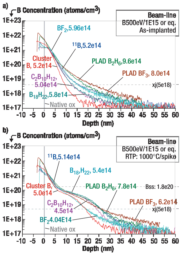 |
| Figure 1. SIMS/ARXPS B profiles of different doping techniques on a) as-implanted wafers, and b) annealed wafers. |
Figure 1 shows SIMS/ARXPS depth profiles of B for different ultra-low energy doping techniques on (Fig. 1a) as-implanted and (Fig. 1b) annealed wafers. The ultra-low energy doping techniques include beam-line atomic 11B implant; BF2, B18H22, C2B10H12 molecular implants; cluster B implant; and B2H6 and BF3 PLAD implants. The implant conditions are B 500eV energy and 1×10¹⁵/cm2 B dose with 0-degree tilt angle or equivalent. SIMS measurement used an O2 primary beam with energy of 500eV and normal incidence. As shown in Fig. 1, the B profile and dose components have been separated. The native oxide thickness is defined and decoupled by ARXPS measurement and shown in Table 1. The B dose values beside the curves in Fig. 1 are SIMS-measured, B retained doses in Si substrate, which have extracted the B loss in the surface native oxides.
C2B10H12 and B18H22 implants show shallower as-implanted profiles and similar annealed profiles and doses as the beam-line atomic 11B implant. The shallower as-implanted profiles are attributed to less channeling effect by the self-PAI effect due to its heavier ion mass. However, self-PAI of C2B10H12 and B18H22 implants could cause more end-of-range (EOR) defects, which causes more profound B transient enhanced diffusion (TED) [17]. Therefore, they show similar annealed profiles with B implant. BF2 implant shows similar as-implanted profile and dose, but shallower annealed profiles than beam-line 11B implant due to the presence of F, which can reduce B TED [17]. Cluster B implants have both shallower as-implanted and annealed profiles due to its self-PAI effect and higher self-sputtering effect [12]. BF3 PLAD shows deeper as-implanted profiles and similar annealed profiles with a relatively poor abruptness than beam-line 11B implant. Similar to beam-line BF2 implant, F species of BF3 PLAD could reduce B TED. B2H6 PLAD shows slightly deeper as-implanted profiles and similar annealed profiles with a similar abruptness with beam-line atomic 11B implant. Because the PLAD processes can have an in situ B-deposited film during implant and have less direct ion bombardment on Si surface [12], this feature could be beneficial to the device performance improvements [8,9] due to immunities of the channeling effect and fewer damages, including the surface and EOR damages, and, in turn, retarding TED effect and reduce leakage. It is noted that both B2H6 and BF3 PLAD show relatively higher retained B dose in Si and with much higher (>4–5 times) B concentration near Si surface than other beam-line-based implants. These features are attributed to the plasma environment and non-mass separation properties of the PLAD process and could be beneficial to the device performance by reducing the contact resistance or surface depletion [8,9].
Among these different doping techniques, except a higher surface B concentration, B2H6 PLAD demonstrates a best match of the retained B profile in depth with beam-line atomic 11B implant including a similar xj and junction abruptness.
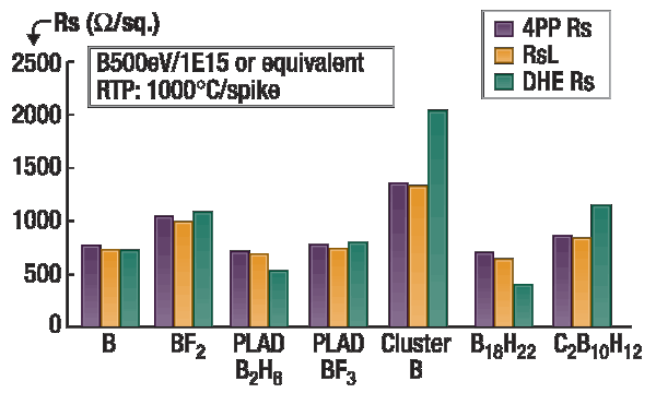 |
| Figure 2. Sheet resistance RS of different doping techniques. 4PP, RSL, and DHE RS are measured by 4 point-probe, non-contact, and CAOT/DHE methods, respectively. |
Figure 2 plots and compares three sheet resistances, 4PP RS, non-contact RSL, and DHE RS, in which 4PP RS and RSL data demonstrate a very good consistency, and 4PP RS, RSL, and DHE RS data demonstrate a fairly good consistency. Cluster B implants show the highest RS due to the higher self-sputtering effect. BF2 implant also shows a relatively higher RS due to its higher self-sputtering and reactive ion etching (RIE) effects. BF3 PLAD and C2B10H12 implants show slightly higher RS. B2H6 PLAD, with beam-line atomic 11B and molecular B18H22 implants, shows the lowest RS.
Self-sputtering effects of these doping techniques are measured separately using the ARXPS technique [12]. Beam-line atomic 11B shows negligible (~0.16nm) self-sputtering effect under its implant condition. Both B18H22 and C2B10H12 show slightly higher self-sputtering effects, but still can be negligible. Cluster B and BF2 implants show significant Si removal (~1.5nm and ~1.2nm, respectively, under their implant conditions) from self-sputtering or RIE effects, respectively. These self-sputtering or RIE effects cause a shallower xj and more B impurity loss so that RS could be higher and saturated. However, the resulting shallower xj on blanket wafer is not a real device xj compared with an SDE baseline of the device structure. For an evaluation of RS-xj characteristics of the device structure, the Si removal by self-sputtering or etching effects must be taken into account. B2H6 and BF3 PLAD processes have no self-sputtering or etching effects, but with little deposition under their implant conditions [12]. The deposition layer can be easily removed by optimized strip and clean processes.
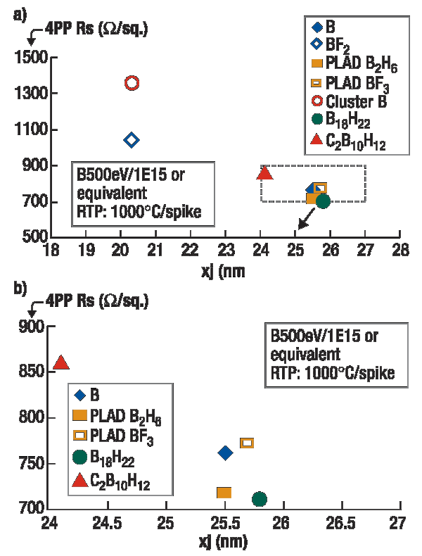 |
| Figure 3. RS-xj characteristics of different doping techniques a) including all doping techniques, and b) excluding BF2 and cluster B implants and zoom-in. |
Figure 3 plots and compares RS-xj characteristics of different doping techniques (Fig. 3a) including all doping techniques and (Fig 3b) excluding BF2 and cluster B implants and zoom-in. The self-sputtering or RIE effects of cluster B and BF2 implants on xj have been taken into account. Among the evaluated doping techniques, B2H6 PLAD and B18H22 beam-line implants show best RS-xj characteristics. BF3 PLAD shows comparable RS-xj characteristics with beam-line 11B implant. C2B10H12 shows slightly worse RS-xj characteristics than beam-line 11B implant. Beam-line BF2 and cluster B show the worst RS-xj characteristics due to their self-sputtering, or RIE, effects.
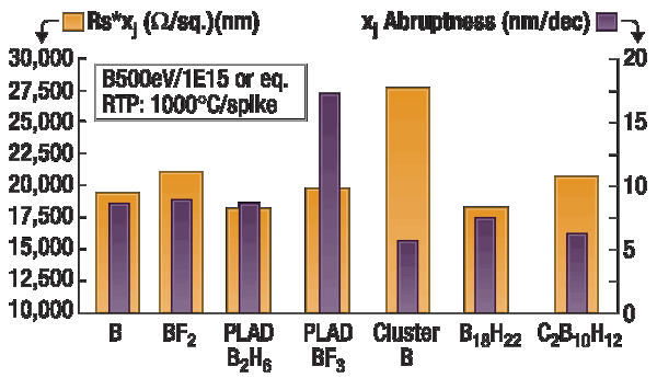 |
| Figure 4. RS×xj product characteristics and junction abruptness of different doping techniques. |
Figure 4 plots and compares RS×xj product and junction abruptness data of different doping techniques. B2H6 PLAD and B18H22 implants show a best RS×xj product with a best trade-off of junction abruptness. Beam-line 11B and C2B10H12 show a fairly good trade-off of RS×xj product and abruptness. Beam-line BF2 shows a reasonable abruptness, but with a relatively larger RS×xj product. BF3 PLAD shows a reasonable RS×xj product, but with the largest abruptness (less abrupt). Cluster B implant shows the lowest abruptness (more abrupt), but with the largest RS×xj product.
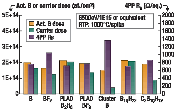 |
| Figure 5. Correlations of 4PP RS versus activated B dose and carrier (hole) dose of different doping techniques. |
Figure 5 plots and compares correlations of 4PP RS versus activated B doses and carrier (hole) doses. Activated B doses are calculated from SIMS profiles by integrating B profiles under boron solid solubility (BSS) level, in which BSS is ~1.8×10²⁰/cm3 at 1000ºC anneal temperature [15].
Carrier (hole) doses are measured by CAOT/DHE method. Good correlations of RS and activated B doses and carrier doses and fairly good consistency between activated B doses and carrier doses have been demonstrated. The relatively larger discrepancies of the consistency between activated B doses and carrier doses on the molecular implants, which have larger and heavier ion species, especially on cluster B implant, have been shown. Such results are apparently due to the heavier ion species implants, which could cause more serious damages and degrade mobility, and the activated B doses do not take the damages into account. B2H6 PLAD and B18H22 implants show the highest carrier doses, which correlate to lowest RS. Beam-line 11B, BF3 PLAD, and C2B10H12 implants show comparable RS and carrier doses. Beam-line BF2 and cluster B implants show higher RS and lower carrier doses due to their serious etching, or self-sputtering effects.
Table 1 lists and compares AFM roughness and ARXPS native oxide data of different doping techniques. All doping techniques show reasonable and comparable surface roughness except the cluster B implant. Cluster B implant shows much larger roughness, ~3 times larger than other implants, which is associated with a serious self-sputtering effect due to its much larger and heavier ion species. Although beam-line BF2 implant also has serious Si etching effects, it shows a comparable roughness because the Si removing mechanism is dominated by RIE of F species rather than the physical sputtering. Native oxide thickness plays a very significant role in ULE implants; not only does it determine impurity loss and final B profiles, but it also impacts the post-implant strip and clean processes. Several factors affect the native oxide thickness. Higher doping level and surface roughness can enhance native oxidation [18]. BF3 PLAD has the highest B concentration peak near the surface and causes thicker native oxide. Cluster B implant has a relatively higher B concentration peak near the surface and has the largest surface roughness due to its large and heavy ion species so that it causes thicker native oxide under the current conditions.
Conclusion
It has been found that B2H6 PLAD and B18H22 molecular implants demonstrate the best RS-xj and abruptness characteristics. Beam-line BF2 implant shows worse RS-xj characteristics due to its serious RIE effect by F species. Cluster B implant shows the worst RS-xj characteristics and very rough surface, which are attributed to its serious self-sputtering effect because of its much larger and heavier ion species. Further optimization may lead to improvement.
Acknowledgments
Additional authors are: Wendy Morinville, Kent Zhuang, Xue-Feng Lin, Chantelle Krasinski and Shifeng Lu (Micron, Boise, ID). Special thanks to Dr. Simon A. Prussin and Mr. Jason Reyes of UCLA for CAOT/DHE measurements.
References
1. International Technology Roadmap for Semiconductor 2008 – Front End Processes, http://www.itrs.net/Links/2008ITRS/Home2008.htm, Semiconductor Industry Association, 2008.
2. J. O. Borland, et al., "Applying Equivalent Scaling to USJ Implantation," Semiconductor International, Vol. 28, No.1, pp. 52-55, 2005.
3. D. Jacobson, "Using Boron Cluster Ion Implantation to Fabricate Ultra-shallow Junctions," The 5th International Workshop on Junction Technology (IWJT2005), Osaka, Japan, June 7-8, 2005, Ext. Abs., pp. 23-26.
4. C. F. Tan, et al., "Performance Characteristics of 65nm PFETs Using Molecular Implant Species for Source and Drain Extensions," Symp. E: Doping Engineering for Front-End Processing, Mat. Res. Soc. (MRS) Spring Meeting, San Francisco, CA, March 24-28, 2008.
5. T. Yamashita, et al., "Formation of S/D-extension Using Boron Gas Cluster Ion Beam Doping for Sub-50nm PMOSFET," The 5th International Workshop on Junction Technology (IWJT2005), Osaka, Japan, June 7-8, 2005, Ext. Abs., pp. 35-36.
6. J. Borland, et al., "USJ and Strained-Si Formation Using Infusion Doping and Deposition," Solid State Technology, pp. 53-58, May 2004.
7. P. K. Chu, et al., "Plasma Immersion Ion Implantation – A Fledgling Technique for Semiconductor Processing," Materials Science & Engineering Reports, vol. R17, no. 6-7, pp. 207-280, 1996.
8. S. Qin, et al., "Device Performance Improvement of PMOS Devices Fabricated by B2H6 PIII/PLAD Processing," IEEE Trans. on Electron Devices, vol. 54, no.9, pp. 2497-2502, September, 2007.
9. S. Qin, et al., "Plasma Doping on 68nm CMOS Device Source/Drain Formations," The 8th International Workshop on Junction Technology (IWJT2008), Shanghai, China, May 15-16, 2008, Proc., pp. 8-13.
10. S. Qin, et al., "Characterization and Optimization of a Plasma-doping Process Using a Pulsed RF-excited Continuous B2H6 Plasma System," Surface and Coatings Tech., vol. 201, no. 15, pp. 6759-6767, April, 2007.
11. S. Qin, et al., "SIMS/ARXPS – A New Technique of Retained Dopant Dose and Profile Measurement of Ultra-Low Energy Doping Processes," IEEE Trans. on Plasma Science, vol. 37, no. 1, pp. 139-145, Jan. 2009.
12. S. Qin, et al., "Comparative Study of Self-Sputtering Effects of Different Boron-based Low Energy Doping Techniques," IEEE Trans. on Plasma Science, vol. 37, no. 9, pp. 1760-1766, Sept. 2009.
13. V. N. Faifer, et al., "Noncontact Sheet Resistance and Leakage Current Mapping for Ultra-shallow Junctions," J. Vac. Sci. Technol. B Vol. 24, No. 1, pp. 414-420, January 2006.
14. S. Qin, et al., "Study of Low-Energy Doping Processes using Continuous Anodic Oxidation Technique/Differential Hall Effect (CAOT/DHE) Measurements ", IEEE Trans. on Plasma Science, vol. 37, no. 9, pp. 1754-1759, September 2009.
15. S. K. Ghandhi, VLSI Fabrication Principles Silicon and Gallium Arsenide, John Wiley & Sons, Inc., New York, NY, 1994, pp. 90.
16. S. Qin, et al., "Comparative Study of Native Oxide Impacts on Low Energy Doping Processes," Jour. of Vacuum Science & Tech. B, accepted and will appear in the Jan/Feb 2010 issue.
17. G. Impellizzeri, et al., "Fluorine in Pre-amorphized Si: Point Defect Engineering and Control of Dopant Diffusion," Jour. of Appl. Phys., vol. 99, 103510, 2006.
18. S. Wolf, et al., Silicon Processing for the VLSI Era, Vol. 1: Process Technology, Lattice Press, Sunset, CA, 1986, pp. 213.
Shu Qin is a senior engineer at Micron Technology, Inc., 8000 S. Federal Way, Boise, Idaho 83707 USA; ph.: 208-368-2144; email [email protected].
More Solid State Technology Current Issue Articles
More Solid State Technology Archives Issue Articles

