|
Executive OVERVIEW It is widely expected that around the 11-15nm technology node, strained silicon may run out of steam and alternative channel materials will be required to achieve the low power performance targets set out in the International Technology Roadmap for Semiconductors (ITRS) [1]. While several grand challenges must be overcome to realize III-V nMOS incorporation in future CMOSFETs, this article addresses three of the most important; improvement of high-k/III-V interface, down selection of junction technology, and co-integration for VLSI using a manufacturable process flow on a silicon platform. |
Richard J.W. Hill, Jeff Huang, Joel Barnett, Paul Kirsch, Raj Jammy, SEMATECH, Austin, TX USA
Traditional silicon MOSFET scaling has driven the majority of the semiconductor industry for the past four decades. In recent years, new materials and processes have been introduced to maintain pace with Moore’s law. High-k gate dielectrics are in volume production and stressor technology is extending the performance of the silicon channel to its limits. III-V materials are widely regarded as leading candidates to fill the nMOS performance gap with both III-V and Ge-based channels being considered for the pMOS device [2,3].
 |
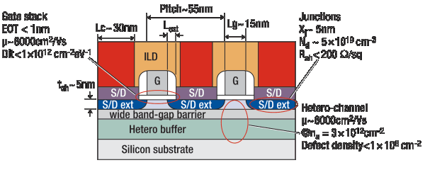
| Figure 1. nFET 15nm technology generation key dimensions and module targets. |
Figure 1 provides a representation of a possible 15nm technology generation nFET. It has a high mobility III-V channel, enabling high performance at low supply voltage. The wide band-gap barrier gives ultra thin body like immunity to short channel effects by improved electrostatic control over the bulk architecture. Heterointegration on a silicon platform is required for III-V integration to be cost competitive.
Gate stack
As III-V materials lack a good native oxide interface, a great deal of research is focused on decreasing high-k III-V interface states. Additionally, there are several other concerns associated with high-k dielectrics. These include Coulomb scattering from bulk oxide charges and interface fixed charges, surface roughness scattering, remote phonon scattering, and dielectric charge trapping associated with reliability problems. These issues need to be understood and addressed concurrently. SEMATECH has investigated:
• the impact of manufacturable ex situ and in situ high-k/higher-k dielectrics;
• conventional process routes and materials such as HfO2, ZrO2, Al2O3 by manufacturable atomic-layer-deposition (ALD) to form quality gate stacks;
• engineering the high-k-channel interface by several means including evaluation of bi-layer schemes to address the dual targets of thin EOT and low Dit;
• defect states and their influence on device properties via detailed electrical and physical characterization and helped in the development of schemes to passivate/eliminate these defects.
 |
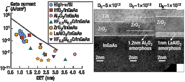
| Figure 2. a) EOT-Jg of high-k/ In0.53Ga0.47As MOS capacitors in comparison with high-k/Si and polySi/SiO2/Si MOS devices; b) TEM cross-section of InGaAs/ALD ZrO2, Al2O3 and LaAlO3 interfaces with mid-gap Dit. |
More specifically, we have addressed key gate stack issues including: a) EOT scalability for high performance and electrostatic control with acceptable leakage current (Fig. 2a Jg ~1A/cm2 @ CET = 1nm), this meets the basic EOT-Jg requirements of a good insulator; b) understanding the source and impact of charge trapping by the insertion of either a LaAlO3 or Al2O3 inter-layer, which reduced the mid-gap Dit by ~5x (Fig. 2b and c) thermal stability on InGaAs [4,5]. The transmission electron microscopy (TEM) images of various ALD gate stacks on InGaAs are shown in Fig. 2b and confirm that the interface is atomically sharp and smooth.
Ultrashallow junctions
In addition to the architecture of the gate region, considerable effort is also ongoing to select the best ohmic contact and junction technology. The physical properties of III-Vs are such that implanted junctions and salicide that have served silicon so well may not be suitable for compound semiconductors. In addition to the challenges that silicon ultrashallow junctions face, implantation of III-Vs suffers from a number of issues including: lower maximum activated doping density, loss of stoichiometry due to preferential group V evaporation, and difficulty in recovering from implant amorphization because of the compound nature of III-Vs [6,7].
A number of alternatives are being pursued as a replacement for implantation as the junction technology of choice. One promising approach is selective regrowth [8]. In this technique, either MBE or MOCVD is used to selectively regrow very heavily doped source/drain regions. This has three distinct advantages over implantation: high doping density, abrupt doping profile and reduced leakage current caused by the absence of implant damage. In addition to providing low parasitic series resistance, regrown source/drains can be used to apply uni-axial strain, further improving performance [9].
 |
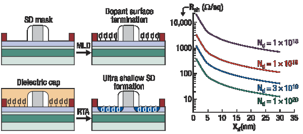
| Figure 3. a) Mono-layer doping process flow; b) SIMS profile after anneals. |
SEMATECH is pursuing a potentially defect-free alternative – mono layer doping (MLD) [10] (Fig. 3a). The III-V surface is terminated by a monolayer of dopant atoms, in this case sulfur, provided from a solution of ammonium sulfide. Other dopant solutions have been demonstrated and the concept could even be extended to ALD or plasma-based schemes. The wafer is then capped with dielectric and annealed. The dopant diffuses into the semiconductor and is activated. MLD has a number of advantages for the formation of ultrashallow junctions: low cost, high uniformity and low damage. Existing toolsets can be used to minimize costs. By terminating the surface with a monolayer of dopant, the exact dopant concentration is known and is self-limiting, allowing for accurate and repeatable junction resistivity. Perhaps most importantly, in contrast to ion implantation, MLD does not introduce lattice damage. Damage determines junction leakage current density, which in turn, controls the device off-state leakage. High mobility III-V materials generally have a smaller band-gap than silicon, which makes them particularly susceptible to high junction leakage, hence, damage-free junctions are a priority in this material system.
Figure 3b shows the extension sheet resistance as a function of depth for various doping densities. The mobility was calculated for each doping density using the empirical model from [11] calibrated by data from internal measurements. For a 5nm junction depth, a Nd >3×1019cm-3 is required to achieve sheet resistance <~200Ω/sq. Although the maximum doping density achieved in III-Vs is approximately an order of magnitude lower than silicon, in the 1019 to 1020 cm-3 range [6], the superior electron mobility >1500cm2/Vs even when highly doped allows low resistance shallow extensions at modest doping density. High Nd is not only attractive to reduce access resistance, but is also required to reduce contact resistance (Rc). When device dimensions and pitch are scaled aggressively (Fig. 1) Rc becomes dominant. When the access length (Lext) is reduced, so is the access resistance, but when the contact length (Lc) is reduced, Rc is increased. At an Lc of 30nm, an Rc of ~1Ωµm-2 is required to meet the parasitic series source drain resistance targets put forth by the ITRS.
Hetero-integration on silicon
A further challenge facing III-V MOSFETs is hetero-integration on a silicon platform. For III-V materials to be considered seriously, the enormous momentum behind silicon manufacturing must be harnessed. III-V MOSFET process flows must use standard silicon technology and must not contaminate silicon lines. Additionally, III-Vs must be hetero-integrated on a large diameter silicon platform to be economically viable. In conjunction with growth partners, SEMATECH is pursuing different technologies to enable high quality III-V growth on Si substrates.
There is a long history of III-V buffer technology development to enable III-Vs to be grown on Si [12-14]. Although thin buffer thickness <400nm would be required for a manufacturable co-integration scheme, thick buffer technology is a convenient interim method to demonstrate the feasibility of hetero-integration and manufacturing compatibility.
 |
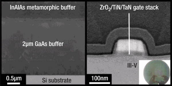
| Figure 4. a) TEM cross-section of the III-V on Si buffer; b) SEM cross-section of a III-V Lg = 140nm device on 200mm Si wafer, with inset photograph of completed III-V on silicon device wafer. |
A 53 % InGaAs buried HEMT structure was grown on a 4

