|
Executive OVERVIEW The introduction of novel gate stack materials (high-k/metal gate) has enabled the resumption of Moore’s Law at the 45/32nm nodes, when conventional Poly/SiON gate stacks ran out of steam. However, different schemes to integrate those novel materials have been recently proposed, traditionally referred to as gate first and gate last. What are the integration options and challenges associated with the integration of such novel materials? What are the main electrical benefits of HK/MG? What is the application range for each of the two approaches. This article discusses these questions and other issues that come to the fore with this disruptive technology. |
Thomas Y. Hoffmann, Imec, Leuven, Belgium
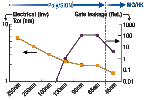
Since the advent of MOS devices over 40 years ago, SiO2 has served as the transistor gate insulator of choice. Electrical oxide thickness (EOT) was scaled at the rate of ~0.7x per generation up to around the 130nm node, but scaling slowed at the 90nm and 65nm nodes as SiO2 ran out of atoms and gate leakage power limited further scaling, as illustrated in Fig. 1 [1].
 |
| Figure 1. Intel’s technology roadmap illustrating how migrating from Poly/SiON to metal gate/high-k (MG/HK) enabled the resumption of electrical Tox scaling, while containing gate leakage [1]. |
HK/MG technology promises to enable conventional scaling of the transistor as well as reduced stand-by power due to a reduction in gate leakage. Taking Intel’s technology roadmap as a example (Fig. 1), switching to HK/MG at the 45nm node enabled to resume the electrical gate dielectric scaling, while reducing the gate leakage by more than 10x.
At the device level, the performance improvement achieved by introducing HK/MG is two-fold. Considering the equation in the long channel approximation (1), the drive current is enhanced with HK/MG through higher gate capacitance, resulting from higher permittivity ε0 of the high-k dielectric over SiO2, along with a scaling of Tinv thanks to metal gate (poly depletion suppression).

where A is the area of the capacitor (WxL), ε0 the permittivity in vacuum.
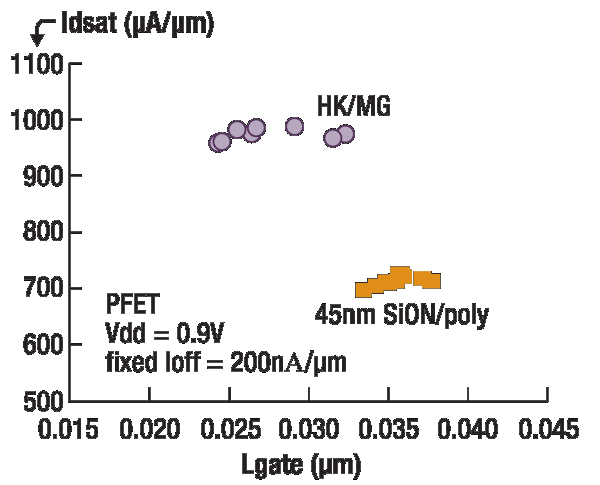
However, performance at high operating clock frequency can be negatively impacted by increased gate capacitance, even if the device drive current is improved. To minimize this penalty when using HK/MG, it is mandatory to concurrently scale down the gate length of the transistor. As shown in Fig. 2 [2], this (minimization of penalty) can be readily achieved thanks to the intrinsically superior electrostatic control of HK/MG over Poly/SiON.
 |
| Figure 2. Electrical Tox scaling of HK/MG over Poly/SiON enables higher drive current as well as Lgate scaling thanks to improved electrostatic control [2]. |
Concerning material options for high-k, extensive research has been undertaken for more than 10 years. Taking into account the many requirements for a gate dielectric (e.g., barrier height, permittivity, thermal stability, interface quality, gate electrode compatibility), a convergence towards Hf-based high-k films (like HfSiO and HfO2) has occurred. However, this is not really the case for the metal electrode, certainly due to the large sensitivity of various processing parameters upon the final effective work function of the gate stack. Among the many candidates, near-midgap nitrided metals like TiN or TaN are arguably among the most common materials considered today.
Possible integration schemes for HK/MG
In the early days of the quest for a HK/MG CMOS solution, a rather disruptive approach based on the complete silicidation of the poly-silicon gate electrode, called FUSI, was proposed [3]. This approach, very promising at first due to its integration simplicity, was abandoned later on due to the difficulty in controlling the silicide phase to achieve low VT devices.
Today, two main integration options remain: gate-first (often referred to as MIPS, metal inserted poly-silicon) and gate-last (also called RMG, replacement metal gate). The terminology ‘first’ and ‘last’ refers to whether the metal electrode is deposited before or after the high temperature activation anneal(s) of the flow.
 |
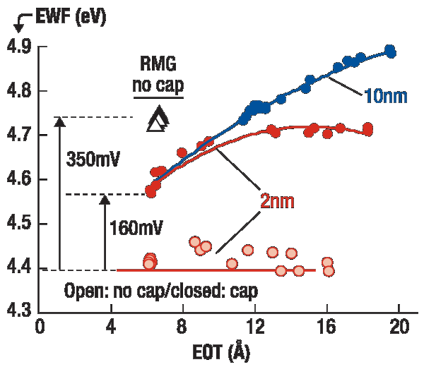
| Figure 3. Effective workfunction (EWF) roll-off towards mid-gap at thin EOT for MIPS, irrespective of the metal gate thickness (2nm or 10nm). |
The gate-first approach was initially developed by Sematech and the IBM-led Fishkill Alliance. It relies on very thin capping layers — Al2O3 for the PMOS and LaOx for the NMOS transistors — to create dipoles that set the threshold voltage of the device. However, thermal instabilities in HK/MG devices were reported and can lead to threshold voltage shifts and re-growth in the gate stack. This issue is particularly acute for pMOS at scaled EOT, as illustrated in Fig. 3 [4]. At those aggressive EOT, it is clear that RMG can deliver significantly higher EWF (meaning lower pMOS VT) than MIPS. Note that this specific issue impedes essentially the use of gate-first for high performance applications. For low power (LSTP) or DRAM applications, where VT and EOT requirements are typically more relaxed, gate-first remains a very viable and promising option for integrating a cost effective HK/MG CMOS solution [5,6].
Nevertheless, significant efforts to enable gate-first for high-performance applications are still under way. One promising work-around to the high VT issue proposed consists in forming by epitaxy a SiGe channel for pMOS devices [7]. This approach intrinsically lowers VT (through valence band off-set) and presents the additional benefit of higher hole mobility than in Si. However, the extra cost associated with this epitaxy tends to offset the process complexity advantage of gate-first over gate-last.
The second way of integrating HK/MG, with a so-called gate-last process, was initially developed by Intel, implementing it in its 45nm technology [1]. In that iteration, the hafnium dielectric was deposited early on in the flow, prior to a sacrificial polysilicon gate was created. After the high-temperature S-D and silicide annealing cycles, the dummy gate was removed and metal gate electrodes were deposited last. More recently, Intel introduced in their 32nm technology a slightly different scheme where the high-k is deposited last, right before the metal gate electrodes, and after the complete removal of the dummy gates. One possible advantage with this new approach is to improve the device reliability and mobility at scaled EOT, which can be significantly degraded when the high-k dielectric has gone through the high thermal steps of the flow, just like in the gate-first approach case [8].
Recently, UMC disclosed a hybrid approach to integrate HK/MG, combining both gate-first (for nMOS) and gate-last (for pMOS) [9]. This allows the tackling of one of the main challenges of gate-first when targeting high-performance applications, which is the high pMOS VT at scaled EOT, while avoiding the full, complex CMOS gate-last integration that requires multiple CMP steps and dual metal gate deposition. Similar to Intel’s 45nm process, this approach is based on a high-k first scheme though, so unless significant progress is being made to improve the thermal stability of the high-k layers, the scalability of this approach to sub-32nm nodes might be difficult. At those advanced nodes, reliability and mobility typically degrade quickly at the target EOT.
One of the concerns often brought up concerning gate-last is its process complexity. As described by Intel [10], the dual metal gates formation involved some critical CMP steps. To maintain sufficient process window, such approach requires more restricted design rules (RDRs), like the 1-D design approach (where gates are all aligned in a given direction). However, at the 28nm node, and more so at the 22nm node, this layout restriction is becoming mainstream anyway, due to lithography constraints. Therefore, the higher design flexibility of gate-first might fade away for the future nodes, as more and more RDRs will need to be implemented.
Looking beyond the 22nm node, the device architecture itself might change from conventional planar to multi-gate (like FinFET or Trigate), in order to improve further the electrostatic control of the device. Those 3D devices might have a significant impact on the integration strategy of HK/MG. Most certainly a CMP-based approach (as in today’s RMG flow) would become extremely complex, if not impossible, making the gate-first scheme the only solution.
 |
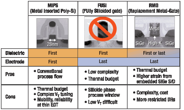
| Figure 4. Pros and cons of different HK/MG integration options. FUSI being abandoned, only gate-first (also commonly called MIPS) or gate-last (or RMG) are actively developed today. |
Conclusion
Today, two main paths to integrate high-k & metal gates, necessary for continuous performance scaling, are actively been developed. The so-called gate-first and gate-last approaches have both pros and cons, as summarized in Fig. 4. For low power applications (which do not require aggressive EOT and ultra low VT), gate-first is arguably the most appropriate choice. However, for high performance applications, complex solutions (like SiGe channel for pMOS) need to be considered in order to meet the performance requirements with a gate-first process. In conclusion, it is quite likely that we will see companies adopting different strategies for the integration of HK/MG, depending on their products portfolio.
References
1. K. Mistry et al., "A 45nm Logic Technology with High-k+Metal Gate Transistors, Strained Silicon, 9 Cu Interconnect Layers, 193nm Dry Patterning, and 100% Pb-free Packaging," IEDM Tech. Dig., pp. 247-250, 2007.
2. K. Henson et al., "Gate Length Scaling and High Drive Currents Enabled for High Performance SOI Technology using High-k/Metal Gate," IEDM Tech. Dig., pp. 645-648, 2008.
3. P. Ranade et al., "High Performance 35nm LGATE CMOS Transistors Featuring NiSi Metal Gate (FUSI), Uniaxial Strained Silicon Channels and 1.2nm Gate Oxide," IEDM Tech. Dig., p. 217, 2005.
4. L. Ragnarsson et al., "Ultralow-EOT (5 Å) Gate-First and Gate-Last High Performance CMOS Achieved by Gate-Electrode Optimization," IEDM Tech. Dig., pp. 663-666, 2009.
5. F. Arnaud et al., "32nm General Purpose Bulk CMOS Technology for High Performance Applications at Low Voltage," IEDM Tech. Dig., pp. 633-636, 2008.
6. T. Tomimatsu et al., "Cost-effective 28nm LSTP CMOS Using Gate-First Metal Gate/High-k Technology," VLSI Tech. Dig., pp. 36-37, 2009.
7. H. R. Harris et al., "Band-engineered Low PMOS VT with High-k/Metal Gates Featured in a Dual Channel CMOS Integration Scheme," VLSI Tech. Dig., pp. 154-155, 2007.
8. K. Choi et al., "Extremely Scaled Gate-First High-k/Metal Gate Stack with EOT of 0.55nm Using Novel Interfacial Layer Scavenging Techniques for 22nm Technology Node and Beyond," VLSI Tech. Dig., pp. 138-139, 2009.
9. C. Lai et al., "A Novel Hybrid High-k/Metal Gate Process for 28nm High Performance CMOSFETs," IEDM Tech. Dig., pp. 655-658, 2009.
10. C. Auth et al., "45nm High-k + Metal Gate Strain-enhanced Transistors," VLSI Tech. Dig., pp. 128-129, 2008.
Biography
Thomas Y. Hoffmann received his PhD degree in 2000 (U. Lille, France) and is director of the FEOL LOGICDRAM research program at IMEC, Kapeldreef 75, 3001 Leuven, Belgium; ph.: 0032-16281894; email [email protected].
More Solid State Technology Current Issue Articles
More Solid State Technology Archives Issue Articles

