by Bob Haavind, editor-at-large, Solid State Technology
March 12, 2010 – The light-emitting diode (LED) market has gone through two cycles of major growth, but an even bigger "third cycle" based on super-efficient lighting looms ahead, perhaps around 2013, predicted speakers at a SEMI breakfast at Teradyne near Boston on March 10.
Jonathon (Jed) Dorsheimer, senior equity analyst for Canaccord Adams, discussed the three growth cycles for LEDs in a talk on the marketplace. High cost and performance issues will limit LED lighting to small specialty niches, he said, until technology and cost reduction make it competitive to alternatives such as fluorescents and halogen lamps. The boom should come about 2013, he predicted, when trigger points and value propositions should be reached in major lighting markets. Even then, as detailed in his firm’s in-depth study to be completed about mid-year, he assumes that external stimulus such as government subsidies and incentives for greener technology would account for 30% of the economic driver sparking a take-off in broad lighting markets.
 |
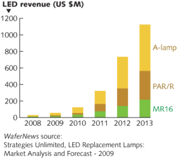
| Available market for LED light bulbs (retrofit lamps). Source: Strategies Unlimited |
The push for green technology will kick-start the coming boom, agreed Chuck DeMilo, director of product marketing for Luminus Devices, an LED company with a fab in Woburn, MA and an assembly facility in Billerica, MA. High-brightness LEDs provide the most efficient lighting source ever, he pointed out, with added benefits including no toxic materials. This is a big plus when compared to the problem of disposing of the mercury in the fluorescent lamps currently replacing incandescents because they are more efficient. Lifetimes of 50,000 hours also offer big advantages. He suggested that while about $50 million worth of LEDs were sold in 2009 to replace lightbulbs, demand will jump to top $1 billion by 2013 as the lighting market takes off.
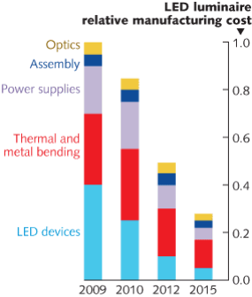
However, cost remains a critical factor. Projections are for a 75% decline in cost for LED devices with a 50% cost reduction at the package level, according to the US Dept. of Energy’s solid-state lighting (SSL) R&D and manufacturing Roadmap, which should open large markets in the lighting sector.
 |
 |
Source: US Department of Energy, Solid-state lighting & research development manufacturing roadmap, Sept. 2009
Dorsheimer showed a $65 bill of materials for an LED lamp, including $25 for the LED itself. This must come down to where a replacement bulb costs about $10, he suggested, before the devices can move into major lighting markets. Currently LEDs are not competitive in commercial and residential lighting where cost/lumen is low. It is expensive to use a 50-foot lift to replace halogen lamps in a workplace such as a factory or warehouse, he suggested. But if light quality is important, such as to add blue sparkle to a diamond in a jewelry display, LED lighting may be favored even with the higher cost.
Enabling technologies, market drivers
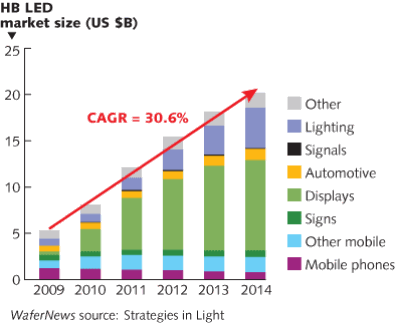
Initial markets for LEDs, including TV remotes and indicators on TV sets, auto dashboards and the like, were the first cycle. The second cycle in the 90s, including color screens on hand sets and blue screens on TV sets, led to overcapacity. Now, even with vendors operating at 40% capacity utilization, Dorsheimer predicts shortages in 2010. The main reason was notebook computers, with LEDs enabling Apple to claim, for example, that its MACs would give eight hours of battery life vs. four hours for a Dell. Going into 2009, LEDs had penetrated 15% of the notebook market; this rose to 75% penetration by the end of the year, he noted.
Now, though, he predicts, undersupply will quickly switch to oversupply, with consequent declines in average selling prices (ASPs) ahead. This will last until about 2013, he believes, when solid-state lighting should be ready to move into major commercial and residential markets.
Dorsheimer gave a cautionary note about the most popular sapphire substrates for epitaxial deposition of LED cells. A shortage of sapphire will constrain the market, he believes, with prices rising some 50%, so he recommended that LED makers stock up now. A lot of the coming cost reduction in devices will come from moving from 2-in. to 4 in. and then 6-in. wafers. The larger substrates will have greater temperature stability across the wafer, increasing the number of in-spec die, even though yields might only be in the 5% range. An in-spec die might bring $0.20, a huge advantage over an off-spec die that might be worth only $0.000002, he explained.
The moderator, Griff Resor, president of Resor Associates, echoed the advantages of going to larger wafers. Since LED devices are much smaller than IC chips, there can be 20,000 of them on a 6-in. wafer, he pointed out.
 |
| Key end-use applications driving HB-LED growth. Long term market-drivers: general illumination and automotive. (Source: Strategies in Light) |
Megatrends driving toward LEDs’ third cycle — including the push for the energy saving of green technology and the steady improvement in LED performance along with cost reduction that could make them viable for wide-scale lighting — has attracted Dow Chemical’s Electronic Materials division. James Fahey, global general manager of growth technologies, identified a broad array of materials problems that could improve processing, device performance, and packaging for LEDs that will be addressed by Dow Chemical. While the processing is simpler than for semiconductors, where Dow Chemical has extensive experience, there still remain many unknowns, Fahey pointed out. But the market potential makes it attractive to tackle these problems and bring improved solutions to the market. The development times for SSL devices is shorter than for semiconductors, he pointed out, where research on a new device may start 10 years before it becomes a commercial product. Many of the LED players in Asia in particular are focused on speed-to-market as well as being very close to customers. Fortunately, R&D costs in LEDs are lower than for semiconductors, he added.
The key enabling technology for high-brightness LEDs is epitaxial growth, but the current state of the art leaves much to be desired, Fahey pointed out. Critical issues include poor wavelength uniformity, long cycle and growth times leading to low throughput, a lack of in-situ monitoring and process control, wafer bow problems, low source efficiency, and incomplete knowledge of growth chemistries and mechanisms.
Improvements and challenges
There is great potential for improvements all up and down the value chain, the speakers agreed, including packaging methods, tools and processes, and device technology. One major hurdle the industry faces is understanding and dealing with "droop" in commercial blue LEDs, which are used in all three methods for creating white light, explained Theodore D. Moustakas, director of the fast-growing Photonics Center at Boston University. At higher current densities, the external quantum efficiency of the devices falls off rapidly. The peak efficiency is at the very low injection level of 20 mA/cm2. Since the effect is related to the current density, larger chips are used for emitters with the same drive current. Finding a way around the droop phenomenon could offer the potential for greater lighting efficiency with smaller devices.
One problem, Professor Moustakas explained, is that there is still disagreement about the science behind the effect. It could be due to polarization effects, or it might be Auger recombination due to high carrier concentrations, creating excess holes and electrons. LED films are deposited on a variety of substrates, and research indicates that nucleation proceeds through the formation and coalescence of hexagonal domains. Threading dislocations through an active device form primarily at these domain boundaries, and this is where the charge leakage occurs.
Another issue in green LEDs is that when more indium is added to strengthen the emission at green wavelengths, the efficiency drops about 10%. If there is a shift from direct bandgap to indirect bandgap in a device, it could help explain a decline in efficiency. But in the case of InGaN green LEDs, the devices remain direct bandgap even when more indium is added, he said, so the cause of the efficiency decline is unclear.
He showed evidence that leakage is much less if ordered rather than random domains can be formed. While gallium and aluminum atoms have approximately the same diameters, nitrogen atoms are about 11% smaller. The threading defects are greater for AlGaN alloys than for GaN. One strategy being tried for ultraviolet LEDs, for example, is to grow devices on AlN substrates to get a more ordered domain structure and fewer dislocations. Another technique for green LEDs is to grow them on a textured GaN template, as shown in work published by Professor Moustakas and others in 2006, suppressing polarization effects and increasing light extraction efficiency.
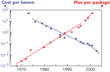
Some companies pushing into LED production are in the semiconductor industry, such as Samsung and Micron, with related processes and similar tools. While the chip industry evolves using Roadmaps based on Moore’s Law, players in the SSL market instead look to an alternate guide called Haitz’s Law, according to Chuck DeMilo of Luminus, which states that every 10 years the light generated by an LED device increases 20×, which the cost per lumen falls by a factor of 10.
 |
| Haitz’ Law: Logarithmic advancements. |
Hundreds of reactors from silicon fabs are being converted to LED work in South Korea, DeMilo said. The complexities of the materials science behind LED production make the transition very tricky, however, suggested Dorsheimer of Canaccord Adams. In fact, he said, some empty fabs are being filled with completely new tools specifically designed for LED processing, though he agreed that many backend tools may be applicable.
Dorsheimer’s analysis showed that 60% of the cost of LED production is in the front-end, and 5%-10% yields are not uncommon. While 40% of the cost is in back-end processing, he said that yields there may be in the 75%-80% range, with the potential to be pushed up toward 95% with process improvements.
While companies coming out of the Univ. of California at Santa Barbara are trying GaN substrates to achieve non-polarized or semi-polarized device fabrication, the cost of these substrates is too high for most commercial markets, Dorsheimer said. He suggested that a 2 in. GaN substrate might cost $2000, and although he agreed higher-quality devices are possible, he is not sure this price will go down enough. If you could achieve 80% of the performance with a sapphire substrate, that may be OK for most markets, he suggested.
Professor Moustakas explained that by going to non-polarized fabrication, quantum wells can be made wider, and the belief of UCSB researchers is that particles can escape from QWs as they narrow at the top.
Alliances and collaboration are becoming much more common in the semiconductor industry, while the LED market has been racked by law suits over intellectual property, according to Dorsheimer. A settlement in 2002 brought five companies together with shared patent licensing agreements. DeMilo discussed how his company had developed a strategic partnership with Nichia in Japan, the largest maker of wafers and phosphors for LEDs. In fact, he explained, Luminus gets its wafers from Nichia, and deconstructs them to fabricate its own devices. Luminus uses a photonic lattice method developed at MIT to fabricate larger chips that can be used as single filaments in various types of lamps. This provides high extraction efficiency, and highly uniform central light, avoiding the shadowing effects created by lamps using multi-chip sources. The optics are also simpler for the big chip approach, DeMilo said.
About a third of the SEMI audience of 70 or so raised their hands when Griff Resor asked how many were already involved in the LED industry in some way. He said he was part of an LED special interest group had been formed by SEMI and commended the program committee for choosing it as a topic. Dorsheimer commented that Applied Materials is moving into this market, and is developing a hybrid-type process for hydride vapor phase epitaxy (HVPE) that might cut processing time for this approach. Molecular beam epitaxy (MBE) and metal organic chemical vapor deposition (MOCVD) also are used for LED film processes.
One member of the audience asked about the potential of organic LEDs (OLEDs) to challenge the nitride devices currently in the marketplace. The panel agreed that OLEDs were in a stage similar to conventional LEDs a decade ago. Dorsheimer suggested that they might fit into some handsets and backplane applications, but he feels they will probably only be a niche player in the market. Some key OLED patents are due to expire in 2017, he added.
More alliances and patent exchanges are likely as the LED industry moves toward its third round of robust growth, the panelists agreed, but the wide range of problems to be tackled will make it an attractive target for those now in the semiconductor processing markets. — B.H.

