by Debra Vogler, senior technical editor, and James Montgomery, news editor, Solid State Technology
March 2, 2010 – Several discussions and presentations at last week’s SPIE Advanced Lithography Conference deserve special note — from work with e-beam EUV mask inspection, to nanoimprint achievements (11nm!), an EUV tool platform roadmap, mask productivity and cost issues at 22nm, and more on SMO and tunable DOEs.
Global Foundries’ joint project with Applied shows feasibility of EBMI for EUV
Obert Wood, principal member of the technical staff at GlobalFoundries, summarized results of a joint e-beam EUV mask inspection project with Applied Materials at the company’s annual Technical Symposium at SPIE (Feb. 24, 2010).
Stating that the e-beam lab setup demonstrated the feasibility of the technology for EUV mask inspection, Wood noted that EBMI (e-beam mask inspection) is a very sensitive option for EUV mask inspection, with increased sensitivity at small absorber pitches. He noted that DUV laser wafer inspection is needed as a complementary method to detect the relatively small number of defects missed by an EBMI or optical mask inspection tool.
Future work includes using Applied’s Aera2 (non-actinic) EUV mask inspection in reflective mode and comparing results to the EBMI and UVision data.
For more on the topic, listen to the podcast interview with Hans Stork, CTO of Applied Material’s Silicon Systems Group.
Samsung’s 11nm NIL success
Engineers at Albany doing imprint lithography on Molecular Imprints’ Imprio-300 tool, showed the following image at SPIE: an 11nm L/S image, taken by Samsung. Thanks to SEMATECH’s Matt Malloy for this image:
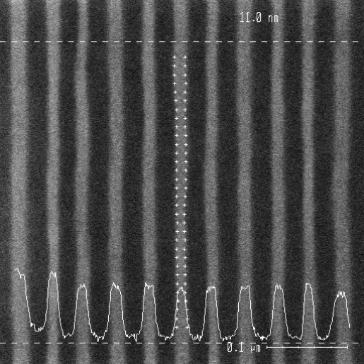 |
| (Image courtesy of SEMATECH and Samsung) |
For more about Molecular Imprints and nanoimprint lithography, listen to the podcast interview with CEO Mark Melliar-Smith.
No EUV for mainstream SoCS? And why DFEB is good
Speaking at the SPIE eBeam Initiative event held in conjunction with , Franklin Kalk, EVP/CTO at Toppan Photomasks, pointed out how masks have become increasingly and dauntingly complex, especially since the 90nm node, with an array of tricks and tweaks. One of the tradeoffs to these extensions of 193nm technology is productivity — aggressive optical proximity correction (OPC), for example, increases e-beam shot count by >10×. (D2S researchers have said e-beam shots must instead be reduced by an order-of-magnitude to make EBDW throughput practical for maskless SoCs.)
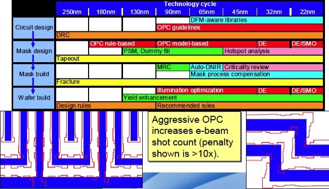 |
| The 22nm challenge: Complex mask shapes required |
The other tradeoff, relatedly, is mask costs. Productivity (line output) and capital costs have been heading in opposite directions for a long time (output lower, costs soaring), and this is especially glaring in the past few nodes. At 22nm, a per-mask capital cost would be ~$60K.
Ultimately, Kalk explained, EUV is likely to be too expensive for mainstream SoCs. Therefore, extending 193i lithography is critical.
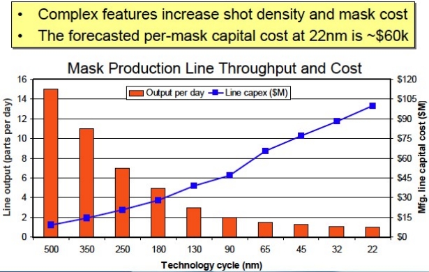 |
| The 22nm challenge: Complexity -> Mask write time -> cost |
Kalk said that critical layer masks should be written in 8-12 hours to be economically viable. He concluded that the proposed design for e-beam (DFEB) masks are good for merchant mask makers.
For more about EUV infrastructure and when it will be ready, listen to the podcast interview with Franklin Kalk.
ASML’s layer-by-layer EUV approach, and an EUV tool roadmap
Christian Wagner, director of product management, EUV, at ASML, tells SST‘s Debra Vogler how the company anticipates the layer-by-layer insertion of EUV into production.
ASML also provided SST with a look at its EUV product roadmap for the Twinscan/NXE platform.
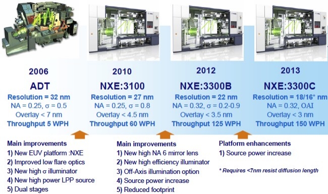 |
| ASML’s TwinScan EUV product roadmap, on the NXE platform. (Source: ASML) |
For more about ASML and EUV, listen to the podcast interview with Christian Wagner.
The skinny on SMO, DOE
James Carriere, senior optical engineer at Tessera, discussed increasing process windows with SMO and customized free-form illumination sources with SST‘s Debra Vogler. He also describes tunable diffractive optical elements (DOE) and how they can be used to create hybrid patterns.
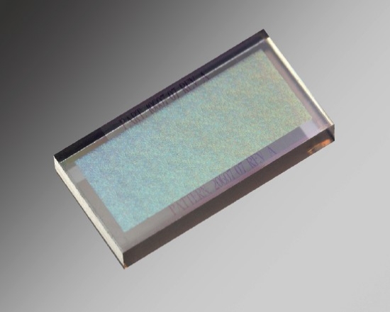 |
| An example of the diffractive optical elements that are used to produce off-axis illumination in lithographic scanner systems. The required phase structure is etched directly into the glass substrate, creating an element that is extremely resistant damage from the excimer laser. |
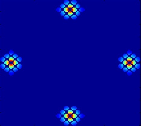 |
| The output from a diffractive optical element is typically specified by a ~200×200 array of pixels with 256 discrete grey levels for 107 degrees of freedom in the design of SMO sources. This quadrupole shows just how flexible the output can be both in resolution as well as pixel energy level. |
For more about this topic, listen to the podcast interview with James Carriere.

