by Debra Vogler, senior technical editor
April 28, 2010 – FEI Company has introduced its Helios NanoLabx50 DualBeam Series (450(S) and 650) that integrates the company’s extreme high-resolution scanning electron microscope (XHR SEM) with a new, high-performance focused ion beam (FIB). Applications for the new system include failure analysis, 3D nanoscale characterization, prototyping, etc., in semiconductor and materials science R&D.
Key to the system’s SEM capabilities is being able to use low voltage (i.e., a more surface-sensitive beam) while achieving a high-resolution image. Degradation of resolution when going to a lower beam energy is avoided by using a monochromator (introduced two years ago) in the XHR SEM, which reduces the energy distribution at the source (i.e., less of a chromatic aberration effect), according to Richard Young, technology manager in FEI’s electronics group. So the spot size of the beam is "tightened" by using a narrower range of electron energies, resulting in a higher resolution, surface-sensitive beam (i.e., at 1kV). In effect, he explained, there is a tradeoff between penetration depth of the electrons and their surface sensitivity.
 |
  |
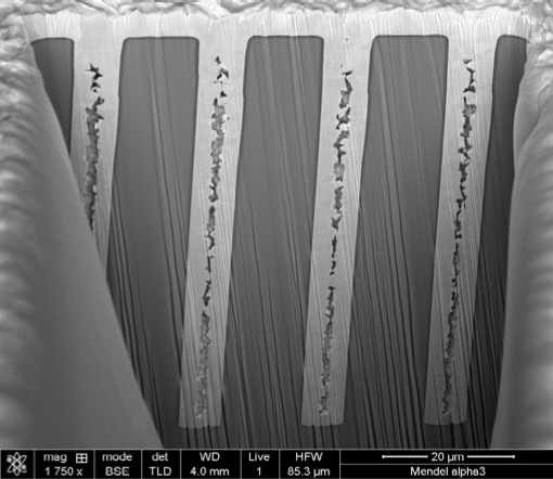
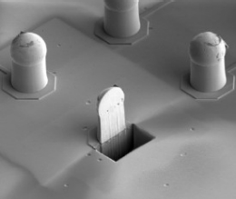
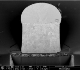
| Figure 1. TSV and interconnect applications. (Source: FEI Co.) |
The XHR SEM imaging is capable of sub-nanometer imaging from 30kV down to 1kV and <1.2nm at coincident WD. Through-silicon vias (TSV) and interconnect applications are challenging because of the increased milling time required for the larger structures. To address this issue, the company’s Tomahawk FIB, which was improved with a fast-switching technology, provides SEM and FIB live monitoring of milling operations, a smaller FIB spot for more precise milling control, and higher beam currents for faster material removal on large structures, such as TSVs (Figure 1). According to Todd Templeton, product marketing manager at FEI, overall throughput of advanced TEM lamella preparation has been improved by 40%. The FIB column is capable of maximum material removal rates at 65nA. In the TSV structures shown in Fig. 1a, a TSV that was 60-80μm deep would take ~12hrs to mill the volume away with the previous tool; with the new tool, however, the time is~4 hrs.
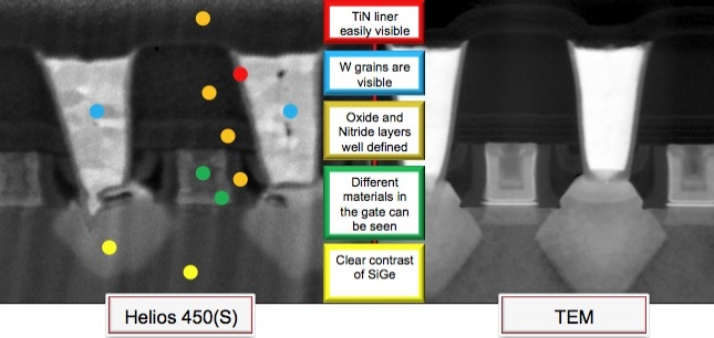
Templeton also told SST that the improved materials contrast of the new platform enables end-users to find defects in cross-sections using the SEM that previously might have to be examined using TEM. "The SEM image (Figure 2, left image) is good enough for many applications for finding defects and process issues," explained Templeton, so "there is no need to go to a TEM image (Fig. 2, right image)." This is beneficial because acquiring the SEM image takes less time than generating a TEM image. However, when a TEM image is required, the new system is capable of handling a higher volume of samples.
 |
| Figure 2. Improved materials contrast in cross-section. (Source: FEI Co.) |

