April 26, 2010 – European R&D consortium IMEC recently offered more details of its work in Ge-on-Si and other novel materials, in efforts to improve two processes: optimizing chemical mechanical planarization (CMP), and improving epitaxial growth using hydrogen and "inert species."
CMP for Ge, III/V materials
Researchers in Europe and the US claim are forming a collaboration to study fundamentals of and optimize chemical mechanical polishing (CMP) for novel materials such as Ge and III/V compounds.
The joint work between European R&D consortium IMEC and Clarkson U.’s (Potsdam, NY) Center for Advanced Materials Processing (CAMP), addresses the need to explore new materials in further scaling of IC devices, e.g. Ge (strained) or III/V compounds for high-mobility channel materials in pMOS and nMOS devices, respectively. Such materials are integrated onto bulk Si wafers after shallow-trench isolation (STI), selectively growth within the trenches through epitaxial processes. The trenches are filled until the material overflows the edges; CMP is thus required to remove the overfill and smooth the surface.
Integration of these novel materials on bulk Si is ongoing, and first CMP processes have been developed, but there is still a need to better understand and then optimize how the CMP processes work, IMEC notes. For example: removal rates should be tunable for Ge and SiO2, where the CMP process must stop; and polished Ge surface after CMP must be defect-free and with very low roughness (<0.5nm root mean square).
 |
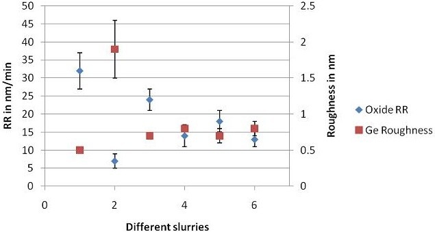
| Oxide removal rate and Ge roughness for various slurries. The oxide removal rate and the Ge roughness are inversely proportional. Source: IMEC |
Thus the IMEC-CAMP collaboration aims to improve the understanding of these materials’ polishing mechanisms. Common understanding of Ge CMP is oxidation of Ge by a strong oxidizer, followed by abrasion of the oxidized Ge layer by abrasives in the slurry. Experiments on Ge disks and Ge-on-Si wafers examining the influence of different oxidizers at various pH values have already yielded a first finding, they report: the oxide removal rate and Ge roughness are inversely proportional, and further tests are planned to explore this correlation.
H2, inerts improve solid-phase epitaxy for Ge-on-Si
IMEC also is summarizing its recent work (published in Applied Physics Letters, in March 2009 and updated in Feb. 2010) in solid-phase epitaxy (SPE) of Ge-on-Si, noting how it can be "a valuable alternative" to conventional heteroepitaxial growth.
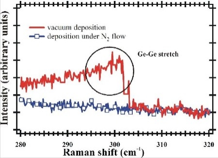
The presence of hydrogen at low temperatures, and/or inert species, they say, "significantly improves the quality of the Ge layers," which have resulting "excellent crystalline quality and low surface roughness" (0.4nm root mean square). In SPE, an amorphous layer is deposited on a crystalline substrate: e.g., using plasma-enhanced chemical vapor deposition (PECVD) with GeH4 or ultrahigh vacuum deposition (UHV). The presence of hydrogen, IMEC says, lowers the surface mobility of adsorbed Ge atoms, increasing the disorder of the deposited layer — which is beneficial to SPE where crystallization starts at the interface first. (Atomic hydrogen is also incorporated in the growing layer but does not affect crystallization, they note.) Similarly, fluxes of H2, N2, or other chemical inert species added during deposition by UHV also reduce surface mobility and thereby the structural ordering of the Ge layers.
Ge deposition is performed at low temperatures (typically 150°C), with crystallization done by thermal annealing (600°C in N2 atmosphere for 1min, though as low as 400°C can be applied). Annealing the structure initiates crystallization at the interface, continuing toward the surface — thus an epitaxial layer can be formed on the substrate. Conventional heteroepitaxial growth would require additional steps to reduce surface roughness, they note.
 |
|
Comparison of Raman measurements of Ge layers deposited in vacuum (red, |

