by David Redinger and Karl Manske, 3M
Executive overview
 |
 |
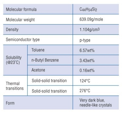
| Figure 1. TIPS_pentacene comprises dark blue, needle-like crystals that form 2D molecular stacking suitable for OFET. |
The potential for chameleon-like fabrics that adapt to changing surroundings, e.g., electronic paper with embedded video, ultra-thin, flexible information displays able to conform to architectural contours, is exciting to say the least. But their development has long depended on the availability of semiconductors able to bring smart functionality to everyday materials at an affordable cost. This article describes one solution that may help spur the next generation in electronics design a fabrication.
April 16, 2010 – Commercial-scale soluble organic pentacene-based semiconductors were recently introduced by 3M working jointly with Outrider Technologies, LLC. The material, 6,13-bis[triisopropylsilylethynyl] pentacene, or TIPS pentacene (Figure 1 and Table) has shown good performance in organic thin-film transistor (TFT) applications. Equally important, the material has demonstrated its compatibility with relatively low-cost, solvent-based processing techniques such as spin coating, spray coating, and dip coating, as well as printing technologies such as ink-jet printing, under full-scale production conditions.
Highly-engineered solutions
Thin-film TFTs built using organic semiconductors operate at slower switching speeds than silicon or GaAs-based electronics, and are not considered a substitution for traditional devices. However, with performance in the range of amorphous silicon thin-film transistors, they are fast enough to drive information displays and similar applications of low to moderate complexity. In addition, the amenability of organic semiconductors to solution deposition and modest process temperature requirements greatly enhances the choice of deposition substrate and affords the opportunity for lower cost products of unique and novel form. To many, they represent the opportunity to bring computing power into every facet of daily life.
The ideal organic semiconductor is one in which mobility is optimized while allowing transistors and other active devices to be fabricated onto flexible substrates using relatively low-cost solution-deposited techniques. "Small molecule" organic semiconductors, such as pentacene, have long been considered excellent semiconductors in their pure state, but their low solubility typically requires vapor deposition, increasing the cost of fabrication. Polymeric semiconductors, in contrast, can be deposited using more economical solution-processing, but they generally offer lower performance.
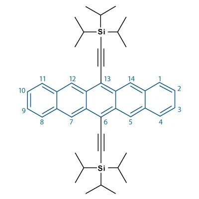
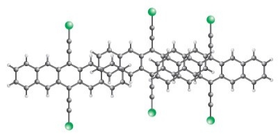
Now, work performed by Prof. J.E. Anthony, University of Kentucky, and founder of Outrider Technologies, has demonstrated that silylethynyl substitution at the 6 and 13 carbons on the pentacene ring system dramatically enhances solubility of this small-molecule semiconductor. Moreover, the substitution favorably impacts molecular alignment. Anthony and his team demonstrated that the silylethynyl substitution encourages a one-dimensional "slipped stack" or a two-dimensional "brickwork" alignment (Figures 2 and 3), increasing the Π-overlap and interface between molecules. Researchers have demonstrated that materials exhibiting the two-dimensional Π-stacking yield the best performance in field effect transistor (FET) devices [1]. Of these substituted materials, TIPS pentacene has proven to be quite successful and is one of the most intensively studied soluble pentacenes.
 |
| Figure 2. 6,13-Bis[(triisopropylsilyl)ethynyl]pentacene. The blue ring in the figure shows the pentacene ring system with carbons numbered. |
 |
| Figure 3. 2-dimensional or "brick-like" stacking arrangement of the TIPS pentacene molecules. |
Fabricating the future
Academic and industry research of organic semiconductors make it clear that choice of solvent, additives, and deposition method are all factors in the ultimate performance of the fabricated devices. Even with the enhanced solubility afforded by silylethynyl substitution, it is not uncommon to utilize solutions that are only one to three percent by weight of TIPS pentacene. Solutions of this concentration are adequate because the final thickness of the deposited and dried semiconductor layer is typically 10-100nm. Rate of solvent evaporation, however, is an important consideration. As reported by Anthony and co-workers, "Subsequent studies of solution-deposited films, where slow solvent evaporation rate allows the pentacene to self-organize during crystallization, showed significantly improved performance in FET devices based on TIPS pentacene, with hole mobility as high as 1.8cm2/Vs observed in films cast from toluene. Careful selection of the casting solvent is critical to yield high quality films and stable device performance [2-4]."
As another consideration, the mobility of an organic semiconductor layer can vary by an order of magnitude depending on the crystal growth across electrodes. This indicates that controlling the crystalline morphology is an important issue when fabricating devices with organic semiconductors. Because TIPS pentacene can be formulated with a number of different additives and tends to crystallize in a favorable morphology, the material can be formulated into semiconductor inks to meet specific applications. For example, when deposited onto a substrate from a blend containing a polymer, TIPS pentacene has been shown to segregate to either the top or bottom of the semiconductor layer, depending on the specific polymer and substrate surface. In a recent study involving a poly(α -methylstyrene)/TIPS pentacene blend spun-cast onto a silica dielectric, semiconductor segregated to the bottom surface of the film, and the resulting TFTs showed mobility as high as 0.54 cm2/Vs [2, 5, 6]. Blends of TIPS pentacene with poly(triarylamine) were more suited to a top-gate device construction because the semiconductor segregated to the top (air) interface. These TFTs afforded mobility as high as 1.1cm2/Vs, with good device uniformity and stability [2, 7].
A number of complex circuits have been developed using TIPS pentacene-based films. Recent studies using solution-deposited TIPS pentacene have demonstrated inverters with a gain of 3.5, using TFTs with FET mobility in the range of 0.2-0.6cm2/Vs. These inverters were then used in seven-stage ring oscillators which operated at >10kHz frequencies. These circuits also operated at voltages as low as -5V [2, 8]. TIPS pentacene has also been used in display backplanes, enabling active-matrix addressing in low-cost, electrophoretic displays. For example, TIPS pentacene has been used in the fabrication of a 10.5-inch, 76dpi display [2, 9]. In addition, TIPS pentacene has been used in an all-inkjet printed electrophoretic display backplane using bottom-gate, bottom-contact devices with an average mobility of 0.19cm2/Vs [2].
Making it real
The introduction of commercially viable TIPS pentacene promises to open a vast field of product development opportunities for designers once limited by the cost and mechanical limitation of silicon-based semiconductors. For example, processing technologies compatible with organic semiconductor formulations would be suitable for printing electronic devices over large areas leading to sheets or perhaps ultimately rolls of electronic paper or smart fabrics.
 |
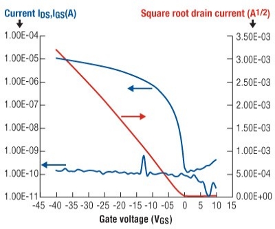
| Figure 4. Typical electrical performance of a TIPS pentacene OFET device. |
Conclusion
While the applications described above are in their design infancy, there are others with a more immediate potential. In particular, radio frequency identification tags (RFIDs) appear to represent a market waiting for an organic solution. Currently driven by silicon chips, RFIDs hold information that can be communicated to a reader as in automated toll booth systems and employee identification badges. Organic integrated circuits would lower the cost-barrier to RFID applications like tagging stock items in warehouses or stores for more advanced inventory control than allowed now by bar codes. Photovoltaics driven by organic electronics is another promising area of application where the potential for low-cost solar cells could spur sweeping changes in markets ranging from energy generation to construction. Information displays for handheld devices, sensors, gauges and other instrumentation are all potential applications where organic semiconductors such as TIPS pentacene can help lower costs and drive smart functionality. Eventually, organic electronics may be as pervasive as their silicon-based counterparts.
Today, however, the learning curve is steep for all involved. New partnerships will be needed as the expertise of chemists, materials scientists, engineers and others versed in interfacial science, coating, and patterning on flexible substrates links with the disciplines of electronic design and fabrication. The first to market will be those who can learn the fastest. Now, with the commercial availability of TIPS pentacene, the race has started.
References
[1]. J.E. Anthony, D.L. Eaton, S.R.Parkin, "A Road Map to Stable, Soluble, Easily Crystallized Pentacene Derivatives," Organic Letters, 4 (1), pp. 15-18, 2002.
[2]. J.E.Anthony, D.E. Vogel, S.M. Schnobrich, R.S. Clough, J.C. Novack, D. Redinger, 3M Corporate Research Laboratories, "Silylethyne-Substituted Pentacenes" (2009) Sigma-Aldrich.com/matsci /a>
[3]. S.K. Park, T.N. Jackson, J.E. Anthony, D.A. Mourey, "High-mobility Solution Processed 6,13-bis(triisopropyl-silylethynyl) Pentacene Organic Thin Film Transistors," Appl. Phys. Lett. 2007, 91, 063514.
[4]. C.S. Kim, S. Lee, S, E.D. Gomez, J.E. Anthony, Y.-L. Loo, "Solvent-dependent Electrical Characteristics and Stability of Organic Thin-film Transistors with Drop Cast bis(triisopropylsilylethynyl) Pentacene" Appl. Phys. Lett. 2008, 93, 103302.
[5]. J. Kang, N. Shin, D.Y. Jang, V.M. Prabhu, D.Y. Yoon, "Structure and Properties of Small Molecule-polymer Blend Semiconductors for Organic Thin Film Transistors," J. Am. Chem. Soc. 2008, 130, 12273
[6]. T. Ohe, M. Kuribayashi, R. Yasuda, A. Tsuboi, K. Nomoto, K. Satori, et al., "Solution-processed Organic Thin-film Transistors with Vertical Nanophase Separation" Appl. Phys. Lett. 2008, 93, 053303.
[7]. R. Hamilton, J. Smith, S. Ogier, M. Heeney, J.E. Anthony, I. McCulloch, "High-performance Polymer-small Molecule Blend Organic Transistors" Adv. Mater. 2009, 21, 1166.
[8]. S.K. Park, J.E. Anthony, T.N. Jackson, "Solution-processed TIPS-Pentacene Organic Thin-film Transistor Circuits," IEEE Electron Dev. Lett. 2007, 28, 877.
[9]. T. Okubo, Y. Kokubo, K. Hatta, R. Matsubara, M. Ishizaki, Y. Ugajin, N. Sekine, N. Kawashima, T. Fukuda, A. Nomoto, T. Ohe, N. Kobayashi, K. Nomoto, J. Kasahara, "10.5-in. VGA All-printed Flexible Organic TFT Backplane for Electrophoretic Displays" Proc. of the 14th International Display Workshop (IDW ’07) 2007, 2, AMD5-4L, 463.
Biographies
David H. Redinger received his BS in electrical engineering from the U. of Illinois at Urbana-Champaign, and his MS and PhD in electrical engineering from the U. of California, Berkeley. He is a senior research engineer at 3M Company, 3M Center, Building 201-1N-34, St. Paul, MN 55144 USA; ph.: 651-733-1128; e-mail: [email protected].
Karl Manske received his BA in chemistry from the U. of Minnesota-Morris and his MS in chemistry from Colorado State U. He is a senior technical service chemist at 3M Company.

