by Prashant Phatak, Imran Hashim, Sandra Malhotra, Sunil Shanker, Wayne French, Hanhong Chen, Pragati Kumar, Edward Haywood, Rick Endo, Tony Chiang, Intermolecular Inc.
Executive overview
With atomic layer deposition (ALD) emerging as a key enabling process for integration of new materials into next-generation process flows, logic and memory developers need the ability to quickly explore the ALD process space. In this paper, we describe the construction and characterization of an ALD process development chamber that allows multiple site-isolated depositions on different quadrants of a 300mm wafer, and also present data from a case study of ZrO2 film development. Both unit film and cell-level electrical data are presented.
May 6, 2010 – Use of ALD for creating well-controlled film stacks has been gaining wider acceptance in the semiconductor industry. Despite its lower throughput and higher cost-of-ownership compared to CVD, even cost-sensitive DRAM manufacturers are choosing ALD because of its ability to deal with scaling challenges such as achieving conformal coverage of high-aspect ratio features while maintaining control of high-k dielectric composition. Moreover, logic and memory producers alike find that ALD provides a level of control on interfaces, doping, and step coverage that is imperative for new-generation applications.
From a process development perspective, ALD’s inherently low throughput leads to long learning cycles and makes identification of optimum processes very challenging. A typical 80Å ALD film can take 3 hours/wafer in a single-wafer tool. In high-volume manufacturing, batch tools are preferred for their higher throughput, but this severely limits the exploration of ALD process space, and can lead to local optimization of baseline processes and materials.
While an ALD unit process that meets composition and/or step coverage specifications is necessary, it is not sufficient for rapid and thorough development of sub-50nm IC technology. The ALD film stack still needs to be integrated into a "cell," which in turn has to meet all the device specifications. For a logic flow, this could be the effective work function of MOSCAP, while for a DRAM flow, MIMCAP leakage/K requirements must be met. With most performance improvements for logic and memory driven by new materials, many of which are deposited by ALD, there is a strong need for a flexible platform that provides fast learning cycles based on much higher throughput.
With that in mind, Intermolecular Inc. developed the High Performance Combinatorial (HPC) AP-30 platform, which integrates 300mm ALD and PVD chambers onto a single mainframe. The HPC ALD chamber offers a 4-8× increase in learning cycle speeds for ALD process development, and has demonstrated success in semiconductor applications such as high-k dielectrics for DRAM. Moreover, learning cycle speed improvements of over 40× have been achieved for MIMCAP "cell" level exploration using a combination of site isolated ALD and PVD depositions.
In this paper, we will describe the unique chamber design that enables multiple site-isolated ALD depositions on different quadrants of a single 300mm wafer. Key elements of this chamber include a unique showerhead design, and a gas purge curtain that enables site-isolated depositions on the same wafer. This will be followed by a case study of ZrO2 film development using the new platform. Unit film data and "cell" level electrical data will be presented.
Chamber characterization
Intermolecular’s 300mm single-wafer TEMPUS ALD chamber is designed for flexibility in process space exploration and identification of globally optimized ALD process solutions. The chamber is capable of isolated deposition in four quadrants, either serially or in parallel; it can also handle full-wafer deposition to validate process scale-up. The chamber incorporates a 400°C capable heater with variable spacing to the showerhead, and is fitted with a fast-response butterfly valve that can be adjusted as a recipe parameter to control the pressure and hence the residence time of precursor and/or oxidant. The chamber can be configured with up to four precursors (solid or liquid, in a variety of sizes) and three carrier gases. It has also been successfully fitted with a direct liquid injection (DLI) system for testing production worthiness of the precursor.
Figure 1 shows the simulation setup and results of site-isolated quadrant deposition. In the simulation, three quadrants of the wafer received Ar flow while one quadrant simultaneously received (Ar + 0.4%N2) gas. Simulation results clearly show that N2 gas is confined to the single quadrant only. Thus, site-isolated ALD can be achieved using an inert gas curtain and balanced gas flow.
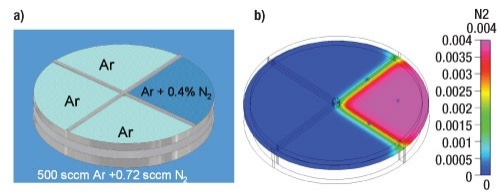 |
| Figure 1. a) Simulation set up for site isolated ALD deposition; b) Simulation results. Note the N2 is confined to a single quadrant. |
Testing on a silicon wafer
Having proven that site-isolated quadrant deposition works, the next step was to test it on a silicon wafer. For this purpose, we performed an experiment outlined in Figure 2a. In this experiment, one quadrant of the wafer received TMA (trimethylaluminum) precursor and H2O oxidant pulses in the following sequence: 1s TMA/10s Ar purge/1s H2O/10s Ar purge. The deposition was performed at 275°C and 1.5 Torr pressure. During the process, the other three quadrants received only inert Ar gas. Before deposition, the 300mm wafer was pre-measured using an ellipsometer to determine the native SiO2 film. After deposition, the Al2O3 film thickness was measured with a 529-point detailed scan. Actual Al2O3 thickness was computed after subtracting the native oxide thickness. As shown in Fig. 2b, Al2O3 deposition was found to be confined to the quadrant that received the TMA and H2O pulses only. Note the sharp boundary between the deposited and non-deposited region. Very little "bleeding" of deposition is observed. Sharpness of deposition can be further optimized by altering the gas flow in the tool. Furthermore, we have observed that the shape of site-isolated quadrant is modulated by precursor properties as well.
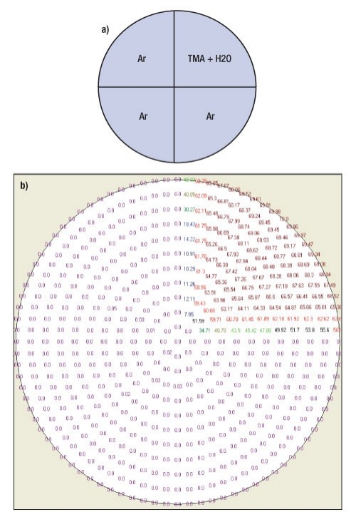 |
| Figure 2. a) Quadrant isolation experimental schematic; b) Thickness map of Al2O3. Note deposition restricted to a single quadrant. |
Next we will illustrate two modes of operation of this chamber. Figure 3 shows the 3D thickness map of Al2O3 deposition on a 300 mm Si wafer using a process similar to the one described above. In this process, sequential deposition of Al2O3 was carried out on each quadrant while the other three quadrants received Ar gas purge. An identical deposition process was used for all four quadrants. The thickness map shown in Fig. 3 again confirms site-isolated ALD deposition in all quadrants. These depositions are separated by a "street" where no deposition takes place.
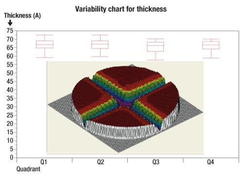 |
| Figure 3. Thickness map of Al2O3 deposition in four quadrants in a sequential manner overlaid on the variability chart. |
A variability plot overlaid on the 3D thickness map confirms that the Al2O3 film has nearly identical thickness in all four quadrants.
The HPC-ALD chamber can also be operated in a "parallel" mode which results in a significantly shorter cycle time, thus enabling more cycles of learning for process exploration. In this mode, all quadrants simultaneously receive the reactive gas pulses for at least part of the process. Figure 4 shows the schematic of such a process, which is extremely useful for depositing films with different thickness in each quadrant. The thickness information can further be used to determine growth rate and/or electrical properties, such as current density vs. EOT plots of a given MIMCAP (metal-insulator-metal capacitor) system. This will be shown in the application section.
 |
| Figure 4. Schematic of Al2O3 deposition process run in a "parallel" mode. Note that all quadrants simultaneously receive TMA+H2O precursors during the first 40 cycles. |
Figure 5 shows the 3D thickness map and thickness vs. cycles plot for this process. During the process depicted in Fig. 4, all quadrants were deposited simultaneously or in a parallel manner for the first 40 cycles. Then quadrant 1 received purge while others got simultaneous deposition for 20 cycles, after which quadrants 1 and 2 received purges, followed by quadrants 1, 2, and 3. The thickness map in Fig. 5a clearly illustrates the successful deposition with increasing thickness from quadrant 1 to 4. Moreover, thickness vs. cycle plot from this process is linear, with very good fit and a deposition rate of 1.1Å/cycle. In a conventional serial manner, it would have taken 280 cycles to complete this thickness series. In contrast, site-isolated deposition in "parallel" mode accomplished this task in only 100 cycles, which resulted in over 60% saving in time and precursor cost.
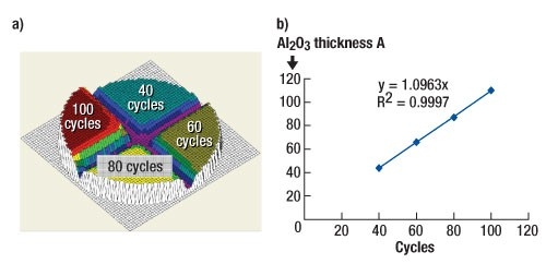 |
| Figure 5. a) Thickness map of site isolated ALD deposition in "parallel" mode; b) Thickness vs. cycle plot indicating growth rate of 1.1Å/cycle. |
DRAM capacitor application example
As mentioned in the introduction, having high-throughput ALD is only a necessary condition for development and integration of the film into production. "Cell"-level data is needed to rapidly validate a film’s production worthiness. For DRAM capacitor dielectric development, in addition to the unit ALD process data, electrical data from MIMCAPs is needed to screen out material or precursor candidates. With this in mind, a study of ALD ZrO2 film properties was carried out using a commercially available Zr precursor, TEMAZ (tetrakis-ethyl-methyl-amido-zirconium). This precursor is being used at the 5Xnm DRAM technology node by many leading memory manufacturers. It has attractive properties such as high vapor pressure, low viscosity, and high reactivity. The main challenge of extending this precursor to the 4X node is its lack of thermal stability.
First, a unit film process was developed using this precursor. Pre-measured (XRF) TiN wafers (TiN/SiO2/Si) were loaded into the ALD chamber and ZrO2 film was deposited using TEMAZ as precursor and O3 as oxidant. Deposited film thickness was measured using XRF and the deposition rate (Å/cycles) was calculated. The XRF tool was cross-calibrated with transmission electron microscopy (TEM) to ensure accurate thickness measurements. Saturation curve for this precursor is shown in Figure 6a. All depositions were carried out with the substrate at 220°C using 10s O3 pulses. The film thickness was seen to saturate after about 5s of TEMAZ pulse, confirming good ALD behavior. Next, growth rate of ZrO2 using TEMAZ was determined from the thickness vs. cycles plot shown in Fig. 6b. For this work, 10s TEMAZ pulses were used. Good linearity is seen with growth rate = 1.44Å/cycle, which is comparable to other published data.
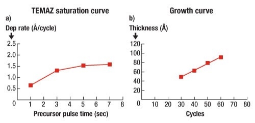 |
| Figure 6. a) Saturation curve for TEMAZ precursor. Good saturation was observed for greater than 5s pulses; b) Growth curve showing linear plot of thickness vs. cycles. Growth rate of 1.4Å/cycle was obtained. |
One of the challenges of TEMAZ is its thermal stability. Decomposition data was collected as a function of substrate temperature to characterize thermal stability of TEMAZ. In this experiment, only precursor pulses are applied to the wafer. Very little film deposition is expected for a thermally stable precursor. Figure 7 shows the thermal decomposition behavior of TEMAZ. It is clearly seen that this ALD window of this precursor is limited to probably <230°C. We have used this insight to develop a more thermally stable precursor with one of its materials partners; data on this material will be presented elsewhere [1].
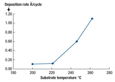 |
| Figure 7. Decomposition behavior of TEMAZ. |
Next, the ZrO2 film was integrated with TiN/Ru electrodes to obtain "cell" level electrical data. ZrO2 film with various thicknesses ranging from 60-80Å was deposited in the HPC-ALD chamber. This was followed by PVD of the Ru top electrode through a shadow mask that defined the size of capacitors (150-500μm diameter). Fabrication was completed with an anneal in an N2 environment at 500°C for 1min using a commercial rapid thermal annealing tool. I-V and C-V characteristics of the capacitors were measured using a CASCADE probe station. Diameters of capacitors were measured using a calibrated optical microscope. From this data, current density at 1V (bottom injection) and equivalent oxide thickness (EOT) was computed. Figure 8 shows the plot of median current density vs. EOT for the MIMCAP structures from four thicknesses of ZrO2 films. Low leakage current density and EOT indicates that high-quality dielectric was deposited using the chamber. Furthermore, K value of ~40 was obtained from the electrical data confirming high-quality crystalline ZrO2 film. These results are comparable to the ALD ZrO2 film data published in the literature [2].
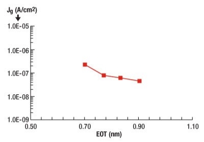 |
| Figure 8. Leakage current density vs. EOT plot of TiN/ZrO2/Ru capacitors. Low leakage and high K (~40) indicates good quality ALD-ZrO2 film. |
Conclusion
We have demonstrated the capabilities of a new platform and in particular, that of the HPC-ALD chamber for rapid process screening and development. The flexibility and high throughput of the ALD chamber allow global process optimization in a much shorter time than traditional methods. This capability is essential for sub-50nm technology development. Moreover, the new platform enables early "cell" level learning that is critical for integrating processes into the production flow. This platform can thus be used for development of a wide range of semiconductor applications such as non-volatile memory, logic, or DRAM.
Acknowledgements
We would like to acknowledge the efforts and contributions of many colleagues at Intermolecular to make this work possible.
HPC is a trademark of Intermolecular Inc.
Biographies
Prashant Phatak received his PhD degree from the U. of California, Berkeley and is account technology director at Intermolecular Inc., 2865 Zanker Road, San Jose, CA 95134 USA; ph.: 408-416-2256; e-mail [email protected].
Imran Hashim received his PhD in materials science from the California Institute of Technology and is senior director of core development programs at Intermolecular Inc.
Sandra Malhotra received her BS in materials science and engineering from the U. of Florida and PhD in materials science and engineering from the U. of Michigan and is a technology director at Intermolecular Inc.
Sunil Shanker received his MS in mechanical engineering from UC Berkeley and is workflow technology manager at Intermolecular Inc.
Wayne French received his BSEET from DeVry University (Kansas City) and is a process engineer at Intermolecular Inc.
Hanhong Chen received his PhD in electrical engineering at Rutgers, the State U. of New Jersey and is senior electrical test engineer at Intermolecular Inc.
Pragati Kumar received his BTech in materials and metallurgical engineering from Indian Institute of Technology (IIT) and MS/PhD in materials science and engineering from Ohio State U. and was formerly a process engineer at Intermolecular Inc.
Edward Haywood received his associates of applied science, electronics engineering technology at ITT Technical Institute and is a process engineer at Intermolecular Inc.
Rick Endo received his BA from Dartmouth College and bachelor of engineering from Thayer School of Engineering and is a director at Intermolecular Inc.
Tony Chiang received his BS in materials science and engineering from Cornell U.
PhD in materials science and engineering from MIT and is the CTO at Intermolecular Inc.
References
[1]. C Xu, et al., "ZrO2 Thin Films Deposited from Novel ALD Zr Precursor for DRAM Capacitor Applications," to be presented at ALD2010 conference.
[2]. J.-H. Kim, et al., "Physical and Electrical Characterization of High-k ZrO2 Metal-insulator-metal Capacitor," Thin Solid Films, 516 (2008) 8333-8336.
[3]. S. K. Kim, C. S. Hwang "Atomic Layer Deposition of ZrO2 Thin Films with High Dielectric Constant on TiN Substrates," Electrochemical and Solid-State Letters, 11 (3) G9-G11 (2008)

