by Jim Blatchford, Steve Prins, Texas Instruments Inc.; Thuc Dam, Linyong Pang, Luminescent Technologies
Executive overview
To reach the 22nm node, most device manufacturers’ roadmaps now include double-patterning (DP) as a means to enable device area scaling with current 193nm immersion exposure lithography tools. As use of DP techniques can add substantial wafer cost, there is a strong desire to limit the number of layers for which these techniques must be applied. Source/mask optimization (SMO) techniques [1] show promise for extending the resolution capability of the single-exposure (SE) approach; however, global optimization of the source and mask together with design rules to date has been challenging. We describe a method, called source/design optimization (SDO) that addresses this challenge.
May 4, 2010 – The 22nm logic node is unprecedented in that it must be realized without the benefit of enabling lithographic exposure tool, so that double-patterning (DP) techniques must be invoked to achieve the resolution requirements. To avoid the potentially high wafer cost associated with extensive use of DP techniques, there is a strong drive to determine design rules for back-end-of-the-line (BEOL) metal and via levels that allow these layers to be manufactured with a single lithographic exposure (SE) per layer. To accomplish this, many device manufacturers are investigating source/mask optimization (SMO) techniques [1] in an attempt to get the most out of the SE strategy. These methods are ideal for tuning an illuminator to optimize process margin for a given collection of pattern layouts; however, design rule development using these methods is generally difficult. In particular, because of computational intensity, these techniques are limited to a relatively small number of layout clips, and choosing the proper clips to represent all possible layout idioms in a given layer can be difficult or impossible. As a result, the optimized illuminator determined by SMO may be a strong function of the clips chosen, and may not give optimal performance for all possible layouts drawn to a given set of design rules.
We describe a systematic method to extract design rules for metal layers while simultaneously performing free-form illumination source optimization, a technique we call source/design optimization (SDO). More detail on this technique can be found elsewhere [2]. The technique leverages the fact that BEOL layers are auto-routed to express the plethora of possible BEOL layout configurations in terms of a handful of rules and pattern templates, upon which SMO can be run.
Analysis
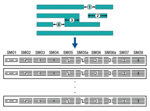
As a precursor to the work, we statistically analyzed large quantities of densely routed 45nm layout, and found that >98% of the structures therein can be represented by the four simple rules indicated in Figure 1. These rules are: the line-end-to-line-end space (indicated by the ‘1’ in the figure), wire length (‘2’), width of the ‘wrong way’ metal (‘3’), and line-end-to-wrong way-metal space (‘4’), as illustrated in the figure. Structures at widths larger than the minimum allowed metal width for a given layer rarely occur, and account for the remaining ~2% of the polygons in the layout. Furthermore, the number of routing tracks spanned by a wrong way-metal interconnect is rarely larger than three.
 |
| Figure 1. Illustration of the four simple rules and construction of the pattern-matching module. |
Based on these observations, we construct a compact ‘row’ of pattern-matching structures that represent the limiting cases for each of the four rules in question, as also is indicated in Fig. 1. As it is general practice in the industry to size up isolated or semi-isolated features to improve process margin, only structures representing minimum values of the four design rules in dense environments (e.g., adjacent to a long metal runner) need to be considered in the analysis. The number of test cases needed to fully describe the limiting cases for each rule is therefore quite small. In the example in question, ten design clips were deemed a sufficient basis set to cover all rule-limiting cases in a typical metal layer.
Once the row of pattern-matching structures is derived for a given candidate design rule set, we then generate a large module containing multiple copies of the row of structures. Each copy of the row is drawn to a slightly different, generally tighter, variation of the four rules, with the last row in the structure pushing all rules to ~70% of their nominal value (based on a simplified illumination optimization). We then execute a standard SMO-like run on this module, using a handful of litho metrics (depth of focus, mask error enhancement factor, line-end pullback) as success criteria, and with the goal of allowing as many rows of the module to pass as possible. We further weight each row based on area impact of the rule changes associated with that row; see ref. [2] for additional detail.
Results
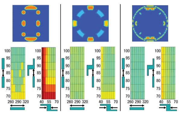
Figure 2 shows some typical results of an SDO run based on a route pitch of 80nm. The left-hand portion of the figure indicates the starting illumination condition based on source mapping techniques (again see ref. [2]). The color plots below the illuminator (hereafter referred to as ‘design space plots’) illustrate the lithographic performance as a function of each of the four rules. Each square in the color map represents a row of the test module, with the nominal (initial) rule values associated with the top right corner of the color plot. Colors ranging from green to blue indicate that all litho metrics are met for that row/rule set. Colors from yellow to red indicate that one or more litho metrics does not meet the success criteria. The center and right-hand portions of Fig. 2 show the optimal parameterized and free-form illuminators for this layer, respectively.
 |
| Figure 2. Comparison of design space performance of an illuminator optimized using non-SDO techniques (left) with two illuminators optimized with SDO (center, right). |
For the left-hand (non-SDO) source, as the design rules are pushed significantly below their nominal values, the lithography margin becomes quite poor, as is indicated by the red and yellow coloring at the bottom left of the associated design space plots. Both of the SDO-derived illuminators show substantially improved performance, as is indicated by the amount of green in the design space plots. For the free-form (right-hand) source, for instance, the critical line-end-to-line-end space and wire length rules can be reduced by ~30% over the values derived from the non-SDO illuminator while still maintaining adequate litho margin. In our calculations of full-chip area [2] using the SDO-derived free-form illuminator, this design space improvement is equivalent to a substantial ~12% reduction in routed area.
Conclusion
The SDO technique is an effective means for jointly optimizing design rules and illumination conditions for auto-routed layers, and can be used to realize significant improvements in overall die area.
References
[1]. See, for example, L. Pang et al., "Considering MEEF in Inverse Lithography Technology (ILT) and Source Mask Optimization (SMO)," Proc. SPIE 7122, 71221W (2008).
[2]. Blatchford et al., "Litho/Design Co-optimization and Area Scaling for the 22nm Logic Node," Proc. of CSTIC, to published in ECS Transactions (2010).
Biographies
Jim Blatchford received his PhD in physics from Ohio State U. and is manager of lithography development and simulation at Texas Instruments Inc., P.O. Box 655012, M/S 365, Dallas, TX 75265 USA; (972) 995-4042; e-mail
[email protected].
Steve Prins received his PhD in electrical engineering from The U. of New Mexico and is Member of the Group Technical Staff at Texas Instruments Inc.
Thuc Dam received his PhD in chemistry from The U. of Texas at Dallas and is global applications manager for North America & Europe at Luminescent Technologies, Palo Alto, CA USA.
Linyong Pang received his PhD in mechanical engineering and additional MS in computer science from Stanford U. and is Sr. VP & GM, computational lithography & inspection at Luminescent Technologies, Palo Alto, CA USA.

