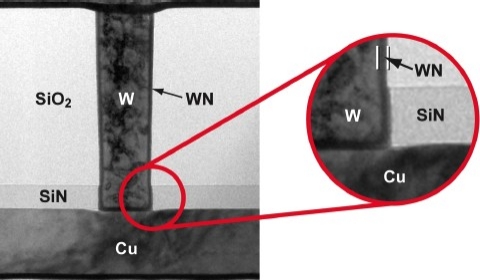
May 10, 2010 – Novellus says it has devised a new process technology for tungsten vias for copper interconnect applications in 3X node and below memory devices.
The "DirectFill" chemical vapor deposition (CVD) tungsten nitride (WN) liner-barrier film replaces conventional physical vapor deposition (PVD) Ti liner and MOCVD TiN barrier film stack used for connecting tungsten vias to Cu interconnects in advanced memory devices.
A common integration scheme for Cu interconnects into flash and DRAM devices incorporates the Cu interconnect for the first metal layer, and traditional Al interconnects for subsequent layers; a tungsten via makes the electrical interconnection between the layers. But shrinking dimensions introduce challenges for this traditional Ti/TiN liner-barrier stacking scheme, which can cause higher via resistance, degraded electrical performance, and poor device reliability:
- Overhang of the PVD-Ti liner reduce the via opening, leading to incomplete CVD tungsten fill and a void in the center of the via.
- MOCVD TiN films are deposited with minimum thickness to prevent silane diffusion through the barrier and formation of high-resistivity copper silicide at the via interface.
- Breakdown in the TiN barrier can result in tungsten hexafluoride attack of the Ti liner, resulting in "volcano" defects.
In Novellus’ new process, an ultrathin (20Å), highly conformal WN film is deposited in a single step (using the company’s Altus platform), with "better" barrier and resistivity properties vs. conventional 200Å thick PVD Ti-MOCVD TiN film stack, the company claims. High conformality of the WN film deposition eliminates step coverage and fill issues with liner-barrier technology; the film’s microcrystalline structure offers a low-resistivity diffusion barrier, eliminating barrier breakdown mechanisms that result in copper silicide formation and volcano defects.
The ultrathin, highly conformal WN film results in up to 30% lower via resistance vs. traditional PVD Ti-MOCVD TiN liner-barrier stack — and thus extends the tungsten via process to and beyond the 3Xnm node, the company says.
 |
| TEM image of a tungsten via in contact with a copper interconnect, with WN film used as the barrier layer. Highly conformal WN film results in void-free tungsten fill and a clean interface between the Cu and W/WN via plug. (Source: Novellus) |

