We haven’t exhausted our technology options — let’s get back to an innovative mindset!
by Joanne Itow, Semico Research
June 4, 2010 – As the semiconductor industry grows its way out of the 2008/2009 downturn, the debate over 450mm wafers inevitably will rear its head again. The major objection to 450mm wafers lies in the research and development cost, and the ability of all parties involved to benefit from the large investment.
 |
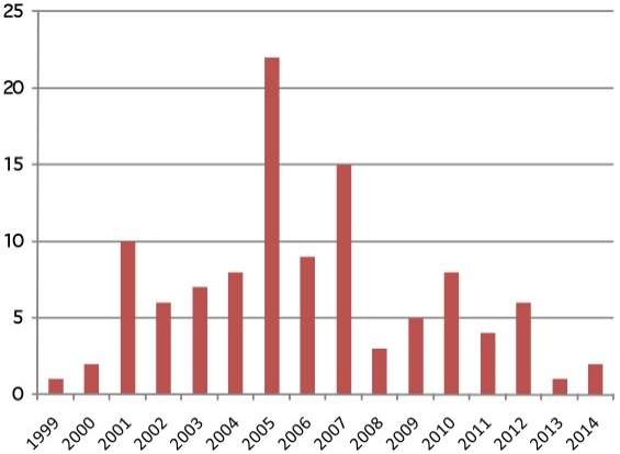
| 300mm fabs coming online by year. (Source: Company sources, Semico Fab Database) |
The industry cannot stagnate at the existing 300mm wafer technology. 300mm wafer fabs have peaked. Based on chip unit volumes, there will be a point where building one 450mm fab will be more cost-effective than building two 300mm fabs. And based on past wafer-size transitions, all semiconductor manufacturers eventually benefit from the productivity improvements and technology options that a larger wafer size offers.
The industry needs to look toward the next manufacturing solution. Consumer demands for more memory will push NAND and DRAM to ever increasing product densities and increased unit volumes. Logic products will continue to move up the performance curve, while offering more features and performance in a system-on-chip or multi-core product.
 |
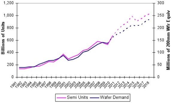
| Total semiconductor units and wafer demand, 1991-2018. (Source: SIA/WSTS, Semico Research Corp.) |
The ability to produce chips on a more economical manufacturing process is good for the overall industry’s future. Availability of low-cost memory and high-performance and/or low-power processors enable the creation of new applications, increasing demand for electronic goods and more semiconductors — a cycle that keeps our industry ticking.
Moreover, the availability of mature capacity enables a plethora of new features. When DRAM vendors moved to 300mm wafers, they used old 200mm capacity to produce cost-effective CMOS image sensors. LED, medical applications, and smart grids are being enabled because of efficient 200mm capacity made available as advanced products move on.
In order to meet our next generation technology demands, the industry will have to find a revolutionary solution. Whether it is 450mm wafers or not, the solution will most likely be expensive and disruptive. But every time an industry executive says we can’t afford the R&D, it sends a discouraging message to all the young, creative engineers: the semiconductor industry is stagnant, protecting profit margins instead of forging new markets.
Competitive markets are designed to weed out the poor performers, but we are weeding out the risk-takers and we’re no longer attracting the best of the young, innovative entrepreneurs. We all need to be sending a positive message that the magic in the black box, whether it is a cell phone or an iPad, starts in the manufacturing of the semiconductor chips.
Joanne Itow is managing director, manufacturing for Semico Research, e-mail [email protected].

