|
Executive Overview An increase in subtle systematic defect mechanisms, smaller feature sizes, and more complex designs make it significantly more time consuming to identify the cause of yield loss using traditional methods. The challenge on the design side is to aim the efforts at the right yield issues. To hit a bull’s eye rather than a black hole with our yield improvement efforts, we can leverage the wealth of information that hides in the manufacturing test results using a technique called diagnosis-driven yield analysis – a technique described in this article. |
Geir Eide, Mentor Graphics Corp., Wilsonville, OR USA
With the adoption of double-digit manufacturing nodes, yield is no longer a challenge just for foundry executives. Driven by demands for shorter time-to-volume, higher mature yields, and strict quality requirements, yield concerns are causing sleepless nights for design, product, test, and failure analysis engineers across the semiconductor industry.
Yield analysis and improvement is often a two-pronged approach. On the design side, ad-hoc techniques, such as redundant via insertion, and systematic approaches, such as design-for-manufacturing (DFM) frameworks [1] and restricted design rules (RDRs) [2], are used to ensure adequate yields. On the post-manufacturing side, yield management systems (YMS) are used along with failure analysis (FA) to monitor the manufacturing and test process to identify when yield problems occur and determine the root cause.
Identifying root cause of yield loss
An investigation is typically initiated when a higher than expected failure rate is observed in manufacturing test. The goal of this effort is to identify the root cause of the excess failures so that a corrective action such as containment (increased test effort), process change, or design change can be taken. Root cause is ultimately determined using physical failure analysis (PFA).
PFA involves a wide range of tools and techniques that aim at locating, characterizing, and visualizing the defect in a failing device. Different techniques are used to identify different types of problems. In addition to being costly and time consuming, many techniques are also destructive.
The critical challenge is to hit the bull’s eye—to select the right devices for PFA and to apply the right analysis methods for the selected devices. The right devices are those that represent the actual yield loss. For instance, assume the expected yield for an established process is 90%. If, for a specific device, actual yield is 80%, about half of the failing devices are likely to represent a systematic issue that needs to be investigated; the other half represents the expected and normal rate of random defects.
There are many potential causes of yield loss, ranging from equipment abnormalities, incorrect handling of the material, and photomask problems, to design and library issues. Many of these issues cause clusters or groups of defective devices on a wafer. A traditional technique for separating devices that have failed because of systematic versus random defects has been to use visualization tools such as stacked wafer maps to look for non-uniform defect distributions.
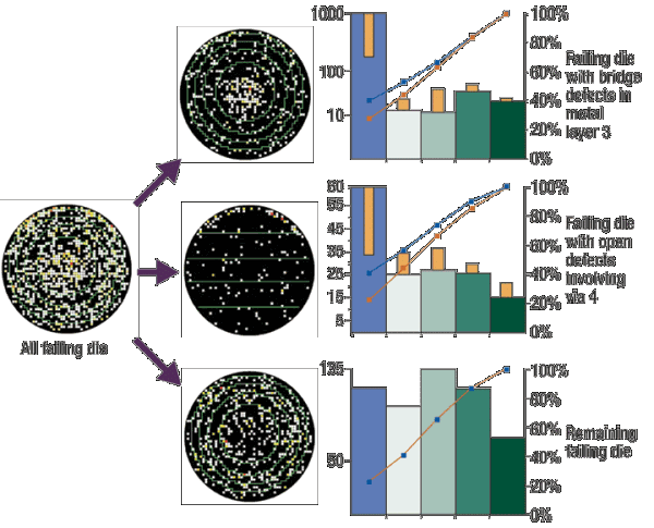
A challenge for complex designs at small process nodes is that this zonal effect can be very subtle, sometimes with multiple fail mechanisms weighing in at the same time, making the bull’s eye very small and thus harder to target accurately. Rather than looking for non-uniform distributions for all failing die, zonal analysis should be based on a finer level of detail. An example of this is shown in Fig. 1.
 |
| Figure 1. While the overall distribution of failing die is uniform, devices with specific types of defects show non-uniform distributions. |
To the left, a stacked wafer map represents all failing die for multiple wafers. An orange-red color represents many failing die in one particular location on the wafer, whereas a white-yellow color represents a smaller number of failing die in that location. The distribution of defects across the die appears to be relatively uniform.
The wafer map in the upper right corner only shows die with bridge defects in metal layer 3. The accompanying Pareto chart represents the number of failing die in five different regions of the wafer; in this case, radial regions starting with the center. There is a much higher concentration of die with this type of defect in the center of the wafer.
The next wafer map shows die with open-defects involving one particular type of via. In this case, there is a significantly higher concentration near the top of the wafer. The third graph shows all the remaining die, i.e., those not part of the other two selections.
To enable this type of zonal analysis, an automated solution is needed to analyze the detailed information, or the "signatures," of each failing die, and statistically test each signature across different sections of material. This identifies groups of die that have an uneven defect distribution. Tessent YieldInsight is a software that specializes in understanding yield loss from scan test data, analyzing more than 70 signatures across 8 different zonal types.
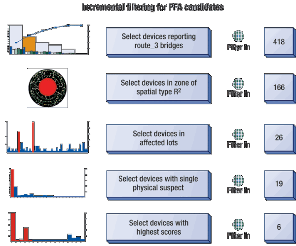
Once a group of devices has been determined to be failing because of a systematic defect, the next step in the process is to target devices for PFA. This can be done by filtering the material based on the most affected portions of the dataset and the devices where PFA is most likely to be successful, as illustrated in Fig. 2.
 |
| Figure 2. Selecting devices for physical failure analysis. |
As a result of this flow, devices that are selected for PFA are known to represent a systematic issue. Knowledge about the specific defect mechanism (such as a bridge in metal layer 3 in a specific location) in these devices helps the failure analysis engineer to know what to look for and what type of equipment to use. This knowledge increases the PFA success rate and dramatically reduces the time to root cause of yield loss.
Zonal analysis has been shown to identify systematic defects effectively. Other approaches, such as correlating failures with DFM violations, also exist. All of these statistical approaches are based on detailed information about multiple failing devices [3]. The most effective way to generate that type of information is through diagnosis.
Enabling effective yield analysis
Scan diagnosis is an established process for localization of defects that also can be used to generate the type of detailed information required for yield analysis.
To simplify the generation of production test patterns, the vast majority of digital semiconductor devices include design-for-test (DFT) structures such as scan chains. In "scan" mode, all sequential elements are configured into a shift register where data can easily be scanned in and out. This makes it easy to control and observe the circuit and facilitates automatic test pattern generation (ATPG). Diagnosis leverages the same DFT structures and ATPG test patterns to determine why a device failed manufacturing test.
The diagnosis process uses the design description, test patterns, and fail information from the tester to identify the location and type of defect most likely causing the failures. Using sophisticated tracing and simulation techniques, the diagnosis tools typically identify a ranked list of suspect defects.
For diagnosis to provide the detailed information needed for yield analysis, more than just the location of the defect has to be determined. For instance, if yield loss is related to one particular type of via5, it is likely that different devices will have defects in different nets.
Assume that there is a problem related to one particular type of via and that, as a result, 50 different devices have defects in 50 different nets. Just knowing the name of the failing net is insufficient, we need to know which metal layers and via types are associated with these nets.
 |
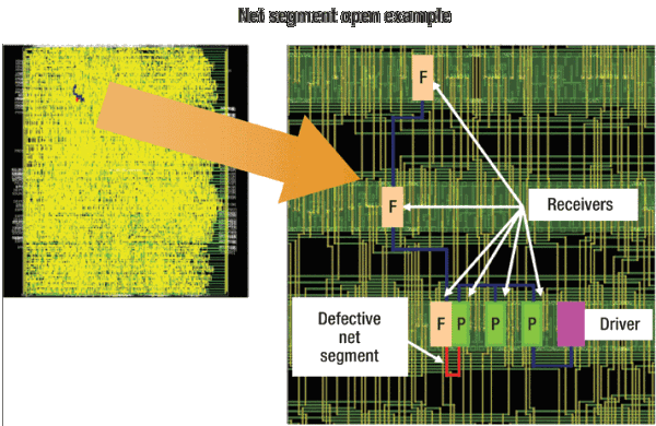
| Figure 3. Layout-aware diagnosis can narrow down the location of an open defect to a net segment by analyzing the net topology. |
This challenge can be addressed through layout-aware diagnosis [4]. In addition to a gate-level design description, layout-aware diagnosis also uses a layout representation. Such a diagnosis process enables a better identification of bridge defects as well as the ability to narrow down an open segment to a segment of a multi fan-out net, as illustrated in Fig. 3. Diagnosis is able to identify which receivers of the net fail and which pass. Based on this type of topology analysis, the defective net segment, and its physical characteristics, such as metal layers and vias included in the segment, can be identified.
Advanced diagnosis solutions such as Tessent Diagnosis can diagnose defects down to a physical polygon, and they can differentiate between defects internal to the cell and defects in the interconnect. These improvements have greatly increased the value of diagnosis in yield analysis.
Diagnosis-driven yield analysis
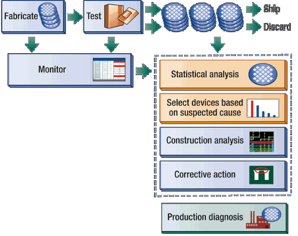
Diagnosis-driven yield analysis is a software approach that combines scan diagnosis with statistical analysis, as shown in Fig. 4. This is a stand-alone solution for analyzing the root cause of yield loss, which also can be used as a complement to other yield improvement approaches, such as in correlating actual failures with DFM and recommended DRC rule violations [5]. This facilitates identification of probable cause of yield loss before PFA and simplifies the device selection. As a result, the PFA success and relevance rates are increased, and the need for costly physical failure localization is eliminated [6].
 |
| Figure 4. In a diagnosis-driven yield analysis flow, diagnosis of production test results is combined with statistical analysis to identify the cause of yield loss and select devices for physical failure analysis. |
Conclusion
An effective diagnosis-driven yield analysis flow can be realized by combining layout-aware scan diagnosis with dedicated statistical analysis. This approach identifies systematic defects and increases PFA relevance and success rates. With a faster time to root cause and the ability to identity yield limiters that may otherwise go undetected, this flow makes it possible to hit the bulls-eye with yield improvement efforts and avoid the black holes.
Acknowledgments
Tessent and YieldInsight are trademarks of Mentor Graphics Corp.
References
1. F. G. Pikus, "Integrated DFM framework for dynamic yield optimization," Mentor Graphics Technical Library, Sept. 2006, http://www.mentor.com/products/ic_nanometer_design/techpubs
2. D. Abercrombie, P. Elakkumanan, L. Liebmann, "Restrictive Design Rules and Their Impact on 22nm Design and Physical Verification," Electronic Design Processes (EDP) April 9–10, 2009. http://www.eda.org/edps/edp09
3. M. Sharma, B. Benware, L. Ling, D. Abercrombie, L. Lee, M. Keim, et al., "Efficiently Performing Yield Enhancements by Identifying Dominant Physical Root Cause from Test Fail Data," Proc. of IEEE International Test Conf. (ITC), pp. 1–9, 2008. www.ieeexplore.ieee.org
4. M. Keim, "Layout-Aware Diagnosis of IC Failures," IC Design and Verification Journal, January 2009. www.icjournal.com.
5. J. Mekkoth, M. Krishna, J. Qian, W. Hsu, C.-H. Chen, Y.S. Chen, et al., "Yield Learning with Layout-aware Advanced Scan Diagnosis," Proc. of International Symp. of Testing and Failure Analysis (ISTFA), pp. 208–418. 2006. www.asminternational.org
6. G. Eide, D. Appello, "The Changing Role of Diagnosis in Yield Analysis," Test & Measurement World, Issue: 11, Dec. 2009, www.tmworld.com
Biography
Geir Eide earned a BS and MS in electrical and computer engineering from the U. of California at Santa Barbara and is a product marketing manager for the Silicon Test Solutions group at Mentor Graphics Corporation, 8005 SW Boeckman Rd., Wilsonville, OR 97070 USA; ph.: 503-685-7943; e-mail: [email protected].
More Solid State Technology Current Issue Articles
More Solid State Technology Archives Issue Articles

