(July 13, 2010) — ASML Holding NV (ASML) announced broad customer adoption of holistic lithography products that optimize semiconductor scanner performance and provide a faster start to chip production. All of ASML’s leading-edge scanners are now sold with one or more holistic lithography components.
Semiconductor manufacturers face increasingly smaller margins of error as they shrink chip features. Holistic lithography provides a way to shrink within these margins to continue Moore’s Law. Introduced a year ago at SEMICON West 2009, ASML’s holistic lithography suite of products enable continued shrink and provide customers with higher yield, sooner. Holistic lithography integrates computational lithography, wafer lithography and process control to optimize production tolerances and reduce “time to money” for chip makers. ASML customers have adopted multiple products from the holistic product portfolio into research & development (R&D) as well as volume manufacturing. Products like Source Mask Optimization (SMO), FlexRay, LithoTuner, Baseliner and YieldStar are in use worldwide.
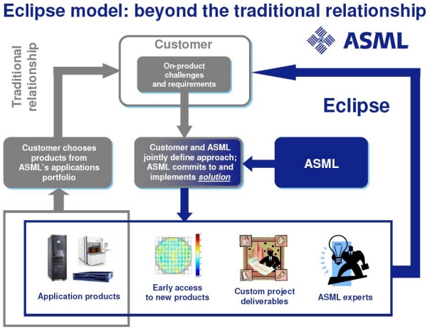
ASML also offers holistic lithography as an integrated package called Eclipse, which is tailored to a specific customer, node and application, and which enables maximum performance at chip making and ramp to volume production at the earliest possible time. A significant number of ASML’s advanced customers have adopted an integrated Eclipse package.
 |
“Most chip makers have found that, for current and future process nodes, independent optimization of process steps is insufficient. The entire litho process must be integrated and co-optimized for the best performance. Eclipse extends the capabilities of their hardware and helps them to produce chips with smaller geometries,” said Bert Koek, senior VP, applications product group at ASML. “With detailed knowledge of our scanner characteristics and interfaces we can work closely with our customers to integrate computational lithography solutions during R&D, and implement customized improvement targets during manufacturing.”
Customers who have adopted Eclipse are seeing the results. STMicroelectronics for example will incorporate Eclipse in conjunction with a TWINSCAN NXT:1950i scanner for their 28-nanometer (nm) node. The key deliverables of the package are on-product specifications for both overlay and critical dimension uniformity (CDU). The 28-nm Eclipse package for ST includes a full range of products from ASML, including scanner tuning products, immersion scanner application, stabilization and conditioning; and the ASML applications support to achieve the specified targets. Preparations for Eclipse at the next node have started with a feasibility study on 20nm critical layer printing options.
“To optimize development cycle times and manufacturing solutions for 28-nm and beyond, ST is working with ASML to define targets, processes and design parameters,” said Joel Hartmann, technology R&D group VP and GM advanced CMOS, derivatives and eNVM technology, STMicroelectronics, at Crolles, France. “ASML’s Eclipse packages include application products, custom project deliverables and application support that enable joint process optimization.”
Holistic lithography approach
The semiconductor industry is driven by shrink that reduces manufacturing cost and improves device performance. However, as semiconductor feature sizes shrink, so do process windows – the accuracy tolerances necessary to produce viable chips – imposing extremely tight requirements on parameters such as overlay and critical dimension uniformity (CDU). Independent optimization of separate parameters is no longer sufficient and holistic lithography intelligently integrates computational lithography, wafer lithography and process control.
During the chip design phase, ASML’s holistic lithography uses actual scanner profiles and tuning capabilities to create a design with the maximum process window for a given node and application. Once in manufacturing, ASML holistic lithography optimizes a scanner for a specific pattern or reticle, and monitors and controls litho-cell overlay and CDU performance over time to continuously maintain the system centered in the process window. Integrated into the Eclipse suite of products are:
- FlexRay uses a programmable array of thousands of individually adjustable micro-mirrors. It can create any pupil shape in a matter of minutes – eliminating the long cycle time associated with diffractive optical element (DOE) design and fabrication and thus accelerating ramp to yield for low k1 designs.
- Tachyon SMO co-optimizes and analyzes scanner source and mask design simultaneously, ensuring an optimized process window from R&D through production while minimizing pitch and number of exposures per layer.
- BaseLiner enables optimized process windows and higher yields by keeping scanner performance to a pre-defined baseline condition.
- YieldStar offers a single sensor solution for CD, overlay and sidewall angle metrology resulting in high-speed, high precision and high-accuracy measurement.
- LithoTuner optimizes the scanner in an application specific manner. By combining device pattern information and scanner specific characteristics, the optimum setting for maximum process window and flexibility will be determined.
ASML provides lithography systems for the semiconductor industry, manufacturing complex machines that are critical to the production of integrated circuits or chips. For more information, visit www.asml.com
See all the latest coverage from SEMICON West at http://www.electroiq.com/index/Semiconductors/semiconwest2010.html

