|
Executive Overview Spacer self-aligned double-patterning (SADP) offers a patterning solution to alleviate the dependency on mask1 and mask2 overlay accuracy in the litho-etch litho-etch (LELE) double-patterning scheme. However, the SADP process sequence introduces additional challenges in defect detection and hence higher risk to production yield. In this work, we developed a methodology to systematically trace the sources of SADP patterning defects by scanning the wafers through consecutive process steps, followed by SEM defect review to identify the major defect types at each step. SEM review was performed at each defect location during the process, and a defect library was established for each step. Our approach and results can be used to develop the inspection strategy during process development and create a defect library to support SADP defect monitoring in production. |
Ofir Montal, Kfir Dotan, Applied Materials Israel, Rehovot, Israel; Bencherki Mebarki, Man-Ping Cai, Chris Ngai, Applied Materials Inc., Santa Clara, CA USA
Lithography resolution gaps at the 32nm technology node and beyond are a natural concern for interconnect manufacturers. EUV lithography is generally accepted as the technology that will succeed 193nm immersion scanners. However, EUV production tools might not be ready in time to meet the production timeline of the 22nm technology node [1]. Hence, several schemes for pitch splitting are being explored to bridge the gap until EUV scanners are ready for production. SADP is considered the leading patterning technology for enabling cost-effective definition of lines and spaces at the 2Xnm node. This approach appears most suited for memory devices, but can be adopted also in logic devices, which use gridded design rules.
As the SADP process consists of multiple deposition and etch steps, it is inherently susceptible to the cumulative effects of defects from each process step. Minimizing this vulnerability requires an extensive defect characterization work to understand defect sources, and optimize inspection strategy for the entire process sequence or module.
In this work we describe a systematic approach to tracing sources and root causes of critical defects affecting 22nm SADP module yield and derive a recommended inspection strategy.
The SADP process
The generic SADP flow [2] is based on the hard mask (HM) stack, core film (APF) deposition followed by litho with relaxed pitch and critical dimension (CD). Then the resist is trimmed to the target CD and the pattern transferred from resist to the core film. The spacer deposition, spacer etch, and core strip and clean steps complete the process sequence. The spacer pattern is transferred to the HM stack used for the specific application. The spacer pattern effectively doubles the line/space frequency and precisely defines the dense lines and spaces of critical layers of memory devices (typically active area, gate and bitline layers). The SADP process is attractive because it involves fewer critical lithography steps compared with other double-patterning schemes. In addition, the CD of the lines to be defined is set by the thickness of the deposited spacer, which is a well known chemical vapor deposition (CVD) process and can be easily controlled to within several angstroms.
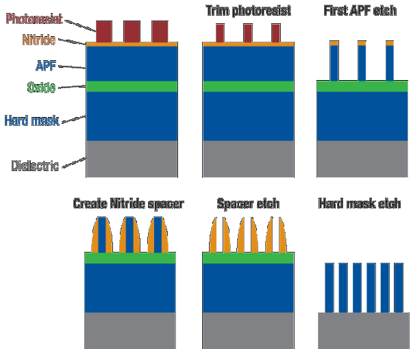 |
| Figure 1. Generic SADP process flow. |
The process flow for the SADP wafers used in this work was developed at the Applied Materials Maydan Technology Center and is shown in Fig. 1.
Double-patterning solutions can be evaluated in terms of the number of process steps involved [3]. While SADP involves the greatest number, it is the most attractive when considering the semiconductor manufacturers’ tight overlay requirements.
Methodology
Several typical patterning defects were used to develop a systematic method of tracing the origin of SADP defects. Wafers from an SADP module were inspected using a polarized deep ultra-violet (DUV) light brightfield (BF) inspection tool [4] and reviewed using a SEM tool.
Detecting small defects at each process step culminating in the 22nm line/space structure requires high sensitivity inspection. A high power, laser-based, DUV BF tool offers this sensitivity by means of a high numerical aperture and small pixel size that reduce wafer noise, high power DUV illumination that enhances scattered light from the defect, and effective scattered light collection.
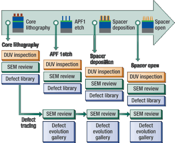 |
| Figure 2. Methodology and work flow for defect characterization and evolution analysis in 22nm SADP processing. |
Wafers were inspected at four different SADP steps shown in Fig. 2: formation of core line/space pattern (core lithography), first core etch (APF1), sidewall spacer deposition, and spacer open (etch and core strip), forming the final 22nm line/space pattern. Recipes were optimized for each inspection step to detect all defect types and sizes. Defect analysis was then performed to characterize the major defect types at each step.
Sets of defects, detected at the first step of the SADP process, were traced and reviewed by SEM in the later process steps to understand their evolution. Defect sources and root causes were analyzed based on their evolution from the first core lithography step to the final double patterning step. The work generated a defect library for each inspected step and a defect gallery illustrating the evolution of a defect over successive process steps.
Results
Our studies showed that exploring defect evolution by tracing defects through the SADP process was an appropriate methodology for defect source analysis and that an optimum inspection strategy could be devised based on this approach.
 |
|
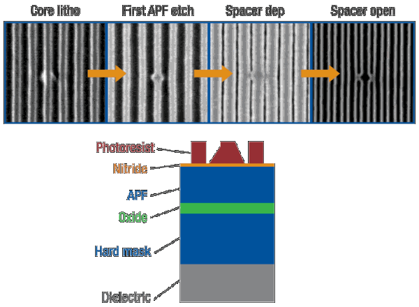
Figure 3. Evolution of defect arising from photoresist scum (top) and schematic of the defect source (bottom). |
Examination of defect evolution revealed that each defect type evolved differently. Figure 3 illustrates defect evolution across the four process steps. Photoresist scum adjacent to the core line sidewalls evolved into protrusions after the first APF etch. Spacer deposition on top of the protrusions caused bridging between core lines. Etch in the following step (core removal) induced a double short at the final 22nm line/space pattern.
This example demonstrates that photoresist remnants at the core lithography step may subsequently lead to full bridging between the double line/space patterns. Inspection following the first photoresist step can reveal such defect issues early in SADP module processing.
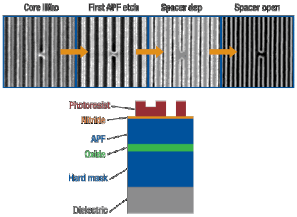 |
| Figure 4. Evolution of defect arising from photoresist bridging scum (top) and schematic of the defect source (bottom). |
Figure 4 presents similar analysis for photoresist scum between the core photoresist lines. This defect leads to bridging after the first APF etch step. Spacer deposition on top of this bridge and etch (core removal) in the following steps leads to the formation of double line cuts and bridging.
These two examples illustrate the potential value of inspection at the lithography step of the SADP module. Understanding defect sources and evolution over successive process steps can offer insights that enable inspection strategy optimization in developing and integrating the SADP process.
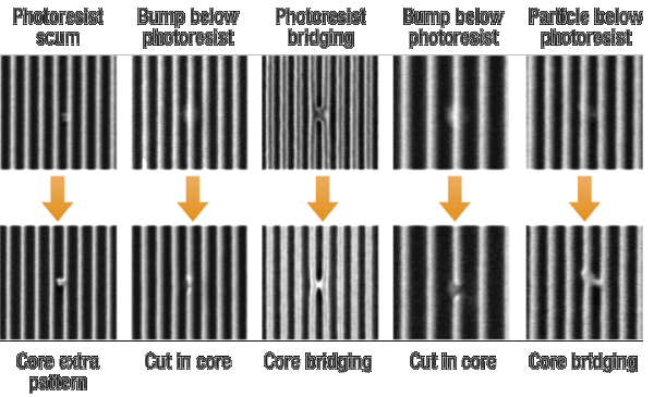 |
| Figure 5. SADP defects gallery, traced at two process steps; photoresist development (top) and first APF etch (bottom). |
Thorough defect evolution analysis was performed for a variety of detected defects. Figure 5 shows defect evolution at two process steps – at the core photoresist development (top) and after the core lines etch (bottom). Both demonstrate the principles of defect evolution: in the first , photoresist scum led to an extra pattern and bridging, while in the second, a particle beneath the photoresist resulted in a narrower line, which broke after the etch step.
Conclusion
In this paper we demonstrated a systematic method for tracing and identifying the origin of SADP patterning defects. This method established a defect library for each of the analyzed process steps and proved suitable for defect source analysis. Analysis showed that most defects detected at the lithography step were likely to continue evolving over the following steps. DUV high sensitivity inspection can detect critical defects at the early stages of processing and is therefore recommended at the SADP lithography step. Tracing defects from the lithography step through the SADP process flow to the spacer open step can significantly increase the capture rate of critical defects at the earlier steps, thereby enhancing interconnect manufacturers’ defect control capabilities and yield.
Deep trench defects, such as deep resist scum and deep polymer residues, were not addressed in this work. Such defects may also have an impact on the electrical performance of the device and are being investigated using DUV BF inspection and SEM review in a manner similar to that presented here.
Acknowledgment
APF is a registered trademark of Applied Materials.
References
1. Vivek Bakshi, Ed., "EUV Lithography," Chapter 3, Wiley Interscience, 2008.
2. C. Bencher, Y. Chen, H. Dai, M. Warren , and H. Lior, "22nm Half-Pitch Patterning by CVD Spacer Self Alignment Double Patterning (SADP)," Optical Microlithography XXI. Edited by Levinson, Harry J. and Dusa, Mircea V. Proc. SPIE, Vol. 6924, pp. 69244E-69244E-7 (2008).
3. A. Conley, D. Meshulach, G. Gichon, I. Dolev, R. Perlovitch, N. Landwer, C. Ngai, Man-Ping Cai, and L. Miao, "From Simulation to Characterization – Integrated Approach for Self Aligned Double Patterning Defectivity", ISSM 2008 YE-O-109.
4. D. Meshulach, I. Dolev, Y. Yamazaki, K. Tsuchiya, M. Kaneko, K. Yoshino, and T. Fujii, "Advanced lithography: wafer defect scattering analysis at DUV," Proc. SPIE, Vol. 7638, 76380K (2010).
Biographies
Ofir Montal received his BSc in electrical and computer engineering from the Ben-Gurion U., Israel, and is a senior brightfield inspection application development engineer at Applied Materials Israel, 9 Oppenheimer St., Rehovot, Israel; ph: (972) 8-9488318, email: [email protected].
Kfir Dotan received his BSc in materials science from the Ben-Gurion U., Israel, and is a senior PDC technologist at the Applied Materials Maydan Technology Center.
Bencherki Mebarki received his PhD in micro-electronics plasma physics from Toulouse U. in France, and is now at Applied Materials.
Man-ping (Cathy) Cai received her MS in electrical engineering from the U. of Minnesota and is a senior defect reduction engineer at the Applied Materials Maydan Technology Center.
Chris Ngai received his BS in mechanical engineering from the U. of California Berkeley and MS from Santa Clara U. and is a director of process and litho engineering at the Applied Materials Maydan Technology Center.
More Solid State Technology Current Issue Articles
More Solid State Technology Archives Issue Articles

