|
Executive Overview Systematic inspection of the front-side, back-side and edge of substrates is becoming more critical – both to provide holistic, 360-degree wafer inspection as well as to increase the productivity and return on investment from today’s multi-billion-dollar fabs. Holistic inspection needs will only increase as the industry continues to drive toward greater cost efficiencies by increasing substrate sizes beyond 300mm diameters to 450mm. This article describes holistic inspection methodology. |
Philippe Gastaldo, Altatech Semiconductor S.A., Montbonnot, France
Advancing the state of the art in IC manufacturing will require new substrates, new materials and greater process integration. For example, creating thin films for the 32nm technology node and beyond will involve large wafer sizes up to 450mm, the integration of new materials such as silicon-on-insulator (SOI) and quartz, epi layers, numerous rapid thermal processing (RTP) steps, and through-silicon-via (TSV) constructions.
At the 32nm node, new types of defects such as crystalline defects from dislocations, pin marks, staking faults and surface pits are generated, which greatly impacts yield. Without a cost-effective means of locating and identifying such faults, the performance of subsequent processing steps will suffer. Lithography performance, which relies on the desired image’s interaction with a substrate’s surface, and TSV technology, which will be used in most emerging high-volume consumer applications, will be affected. A new approach to substrate inspection is needed.
Better information, better judgment
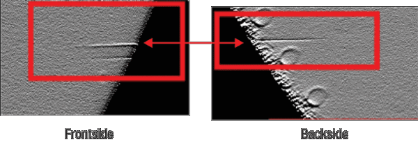
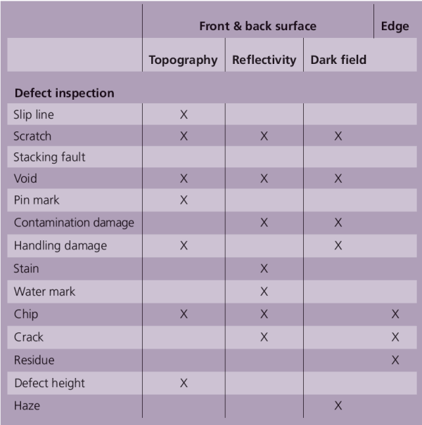
The main goal of any wafer-inspection operation is to search for defects, identify them by type, and pinpoint their location so that process engineers and fab personnel can work to eliminate their causes. With a holistic approach (Fig. 1), the strategy is to extend the effectiveness of defect detection by performing global inspection in a single wafer pass. This requires leveraging the best capabilities of several different inspection technologies in a single tool (Table 1) and using them to generate actionable reports for users. As a result, holistic inspection achieves higher accuracy in defect classification by using complementary technologies, then combining and comparing the collected data to generate accurate maps of all types of defects.
 |
| Figure 1. The combination of front-side, back-side and edge inspection has become critical. |
 |
| Table 1. Combining multiple inspection technologies enables more accurate defect detection and classification |
Two key, complementary defect-detection technologies that work in tandem to form an effective holistic approach are phase-shift and dark-field inspection. Phase-shift inspection enables surface inspection by projecting the intended pattern on a substrate’s surface and then analyzing the reflected picture. This technology is very sensitive to local topography and to any variations in local reflectivity.
Simultaneously, dark-field technology is used to measure scattered light under high-intensity surface illumination. This technology is most suitable in detecting particles and scratches. EyeEdge optical edge-inspection sensors have been developed that provide both high resolution and large depth-of-focus (500µm) to identify defects including chips and film delamination (Fig. 2) at the 100 wafer-per-hour throughputs required in production fabs.
 |
| Figure 2. High-resolution edge images. |
Combining these technologies in an integrated inspection system enables detection and identification of wafer defects generated in today’s Class 10 manufacturing environments that could not be found and accurately classified using any single inspection technology. Finding and correcting these defects can impact yields by up to 18%, as Altatech Semiconductor has found in its work with leading advanced wafer suppliers.
In addition, the broad range of data gathered from holistic inspection makes it possible to conduct a finer analysis of the findings, and thus avoid judgment errors on the criticality of any detected defects. This approach has demonstrated its ability to distinguish between handling-oriented scratches and process-induced slip lines, stains and voids.
Upstream analysis in production
Detecting and classifying defects as soon as they appear allows device manufacturers to quickly perform analysis, determine the root causes of defects, and take corrective measures before manufacturing yields are degraded. Using a holistic approach, defects that might go undetected using one inspection technology can be found by other means. For example, wafer lapping or thinning, cleaving for SOI, and RTP can result in rough surfaces on in-process wafers. These processes can make defect detection difficult for some traditional inspection methods. Indeed, detecting defects of only a few nanometers in size on a rough surface is impossible with scattering analysis techniques or reflectivity measurement. On the other hand, techniques sensitive to nano-topography, with some improvements, are very efficient at finding these problems. Finding defects of all sizes and origins is vital to troubleshooting upstream processing problems.
The right combination for the best performance
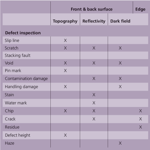
Using a combination of different inspection technologies makes sense only if each of them achieves the desired results in its own field of excellence. Inspection capabilities are evaluated on technical performance, of course, but also on reliability and cost effectiveness. The throughput of a holistic inspection tool must equal or even exceed that of individual inspection technologies (Table 2).
 |
| Table 2. High capture rate with high throughput is mandatory for advanced wafer inspection |
Conclusion
Given the economics of today’s semiconductor industry, a holistic strategy is required to find and correct process-induced defects – especially on bare wafers and engineered substrates and in mission-critical steps such as TSV processing. To achieve their productivity goals and generate return on investment, device manufacturers and wafer suppliers need to apply both phase-shift and dark-field inspection technologies to fully examine the front, back and edges of in-process wafers, and then generate a complete and accurate defect map. This 100% inspection step needs to keep pace with a production flow of 100 wafers per hour.
For the 32nm node and beyond, it has become necessary to take a holistic approach to defect detection. Inspection tools must provide information that is precise, but also global. While defect tolerances continue to shrink, so does the tolerance for missing some defects because of incomplete inspection methodologies.
Acknowledgment
EyeEdge is a trademark of Altatech Semiconductor S.A.
Biography
Philippe Gastaldo received his PhD at Institut National Polytechnique of Grenoble – France and is nanovision director at Altatech Semiconductor S.A., 711, Rue Aristide Berges, 38330, Montbonnot Saint Martin, France; ph.: +33 456 526 800; email Philippe. [email protected]
More Solid State Technology Current Issue Articles
More Solid State Technology Archives Issue Articles

