(July 14, 2010) — Imec and ASML collaborated to qualify ASML’s Tachyon Source Mask Optimization and programmable illuminator system FlexRay, proving its potential with the demonstration of a 22nm SRAM memory cell. In October 2010, the ASML XT:1900i lithography scanner at imec will be equipped with FlexRay, enabling imec to explore the ultimate frontiers of immersion lithography.
A key part of any optical lithography system is the illuminator. It creates the pupil shape, i.e. the condition and shape of the light beam before it hits the mask. By tailoring the pupil shape to the specific layout to be printed, the resolution and process margins can be improved. Optimizing the pupil shape is thus critical, especially with process tolerances reaching the limits of manufacturability.
The use of a customized freeform illumination source shape — optimized for a particular critical chip layout — leads to enhanced imaging results. Early joint development work between imec and ASML compared the use of traditional and freeform illumination modes, and demonstrated convincing improvement in all imaging quality metrics (process latitudes: exposure latitude, depth of focus, mask error factor), and with that also proved clear enhancement in the CD uniformity control over the entire chip and wafer area. Consequently, optimized freeform illumination helps bringing the limits of immersion lithography to areas where traditional illumination modes cannot get, and in that respect enables continued chip feature shrink and faster ramp to volume production, resulting in higher production yields.
 |
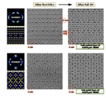
| Figure 1. Double patterning of the contact and metal layer for a 22nm node SRAM of 0.078µm² bit cell area using freeform illumination. |
Freeform illumination has become fully available through ASML’s FlexRay, allowing for virtually unconstrained intensity distribution within the source pupil. FlexRay uses a programmable array of thousands of individually adjustable micro-mirrors to create any pupil shape in a matter of minutes. This is a major advantage over traditional illuminators, which require individual optical elements designed and fabricated specifically for each mask pattern. During FlexRay’s development, imec provided ASML with experimental wafer data that allowed comparing freeform and traditional illumination on a customer test pattern. FlexRay showed excellent performance in terms of pupil control and stability, as well as operational speed, and ability to match to existing illumination modes and other scanners.
Finally, imec proved the potential of freeform illumination with a demonstration of double patterning into a hard mask of the contact and metal layer for a 22nm node SRAM of 0.078µm² bit cell area, with the application of simultaneous source & mask optimization (ASML Brion Tachyon SMO) and imaging using FlexRay illumination. Already from the images, but in particular from the metrics, it is very clear how freeform illumination leads to a pattern quality that cannot be realized using standard illumination. In this particular case, the XY asymmetric position of the freeform poles cannot be mimicked in a standard source.
Kurt Ronse, Director Lithography Program at imec says: “Imec has demonstrated that optimized freeform illumination will help push the limits of immersion lithography. It will create margin that will allow further scaling. To explore this path, and to bring this technology to our partners, we will equip our XT:1900i litho tool with FlexRay.”
Ludo Deferm, IMEC, says that the research group’s focus remains on 3D packaging, advanced lithography, immersion lithography, EUV, mask cleaning, and other projects. Deferm sees immersion lithography as a relevant semiconductor manufacturing technology for longer than some in the industry expected.
Imec performs world-leading research in nanoelectronics. Further information on imec can be found at www.imec.be.
Get all the latest news and interviews from SEMICON West at http://www.electroiq.com/index/Semiconductors/semiconwest2010.html


