(July 16, 2010) — While we were not allowed to snap photos of the proprietary processes inside Applied Materials, Solid State Technology editor in chief Pete Singer put together these photos with information from the Applied Materials tour. Highlights include a solar-panel roof on the parking area, and discussion of AMAT’s new products.
Pete Singer’s Tweets from the Applied Materials Tour:
# What’s new: Centura AdvantEdge Mesa etch system with new ICP source design. 1% etch depth non-uniformity.
# 20th year celebration of Endura. 4500 in the field now at more than 100 customers.
# "New" Endura Avenir system is RF PVD that deposits multiple metallic layers for metal gates.
 |
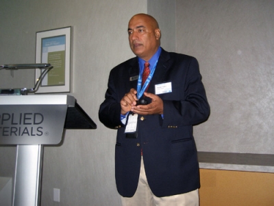
| Randir Thakur speaks to the press at Applied Materials. |
| AMAT’s parking lot is covered with a solar panel roof. |
 |
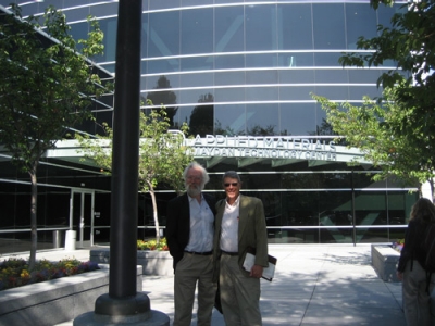
| Dick James, Chipworks, poses with journalist Dave Lammers in front of the Applied Materials building. |
"Precisely engineered" interfaces.
# Thakur (pictured at right) says, "RTP, EPI, CMP, inspection, CVD and PVD tools integrated in MTC."
# Avenir is already "tool of record" for leading logic and foundry 22nm.
# Tablets like iPad key new app driving flash memory. Going to see enormous growth in coming months.
# Products: need to scale platform, have no software problems and deliver on the wafer.
# 50x feature size reduction in last 20 years on Endura.
# 60 of new etch chambers at customers.
# Producer Avila low temp TSV other new product.
# 30k ft2 MTC has 120 tools include full TSV process line.
# April 23, 1990: first Endura. 2000: 300mm. Virtually every microchip in last 20 yrs produced on Endura, says AMAT.
# Avenir RF PVD: capable of 10A layers almost equivalent to ALD. RFPVD = less damage during gate stack formation.
# RFPVD can deposit both metals and metal oxides. Two options: gate first or gate last. First has 3-4 metal layers; Last has 7-8.
# R&D Endura for MG has 7 chambers incl ALD, CVD, RFPVD (3 of the latter).
# Avenir has 87% bottom coverage.
# Avenir: TiN for PMOS and TiAl for NMOS to achieve different work functions. 4.2 vs 4.9 eV.
# Centinel RE-ALD enables thinner diffusion barriers. No chlorine, low temp, halogen-free process.
# Via middle or via last two options: either can be done at wafer fab; via last done at OSATs. AMAT offers tools ‘cept bonding and grinding.
# Sesh Ramaswami: 3D packaging started with cameras then stacked memory, gaming consoles and now networking.
# Post bond-to-carrier processes need to be low temp.
# Competition announced a way to reduce Cu overburden by etch; AMAT says it doesn’t create overburden so no need to remove.
# Thermal budget less than 200°C post bonding. AMAT has doe "quite a bit of integration work" in this area.
# Avila combines throughput and low temp in Producer dual chamber system for isolation liner, backside seal and CMP stop and passivation.
# Isolation liner hermetic comp to 400°C PECVD process.
# RDL passivation process also developed with incl "seamless" passivation of Cu bumps.
# Up to 3× throughput and >30% lower CoO compared to competing systems, says Ramaswami.
# More than 25 customer integration lots have been processed in 2010. Glass carriers also supported.
Sign up for Pete Singer’s twitter at http://twitter.com/PetesTweetsPW
Get more news, podcast interviews, and videos from SEMICON West at http://www.electroiq.com/index/Semiconductors/semiconwest2010.html
Read about AMAT’s 5 new products, listen to a podcast interview about the AdvantEdge Mesa etch system, and watch a video interview about the product launches here: http://www.electroiq.com/index/display/semiconductors-article-display/7651049861/articles/solid-state-technology/semiconductors/industry-news/technology-news/2010/july/applied-materials.html

