July 12, 2010 – Unit shipments of key semiconductor materials are already back to record levels just a year after the most punishing period in the industry’s history, but the growth will slow in 2011 for several reasons, according to the latest forecast data presented at SEMICON West.
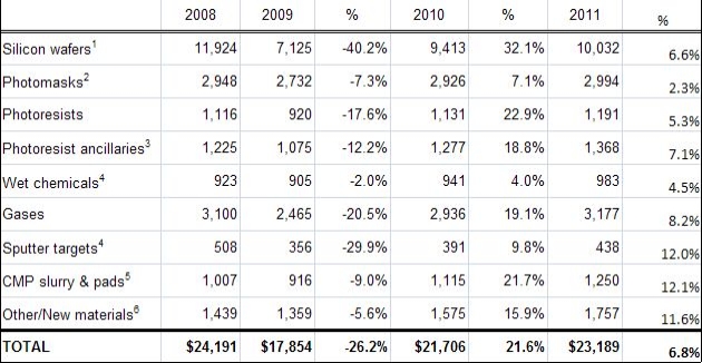
The total semiconductor materials market will grow 21.6% in 2010 to $21.71B (vs. -26.2% in 2009, $17.854B), said Dan Tracy, presenting at the Gartner-hosted Monday afternoon symposium. Look for this to slow to 6.8% in 2011 to $23.19B. (But still not at 2008 levels of $24.19B.)
Best growth in 2010: Silicon wafers (32% to $9.41B), followed by photoresists (23%, $1.13B) and CMP slurry/pads (21.7%, $1.11B). Wafers also represented the biggest turnaround from 2009, when they suffered a -40% decline. Projected 25% growth in wafer unit shipments this year could end up approaching 31%-32%, Tracy said (2Q area shipments were up at least 5% sequentially). There’s demand for 200mm wafers too, as capacity brought offline in 2007-2008 is now being brought back online for analog and discrete use. Even 6-in. wafer demand was up 20% through May, he pointed out.
"Wafer suppliers saw very steep erosion" in the downturn, Tracy pointed out. "They want to regain pricing strength in 2010."
Lowest growth in 2010, in single-digits, will be seen in wet chemicals (4.0%, $941B), photomasks (7.1%, $2.93B), and sputter targets (9.8%, $391B). Others are respectably in the teens.
As things slow into 2010, look for single-digits in the big categories (wafers, gases, photomasks/resists/ancillaries), but around 12% growth for CMP, sputter targets, and other/new materials.

(Source: SEMI)
1 Silicon wafers include merchant sales value only; includes SOI wafers; no reclaim wafers
2 Includes captive market
3 Includes resist removal chemicals, developers, anti-reflective coatings, contrast enhancers, edge bead removers, adhesion promoters, etc.
4 Source is Techcet Group LLC, includes precious metals
5 Estimates for IC applications only
6 Includes low-k dielectrics, copper plating solutions, dielectric precursors, organometallic precursors, etc.
Narrowing in on specific segments:
Photoresist chemicals. SEMI projects 23% growth in this segment in 2010. 193nm resists, which make up 40% of the market, will reach $450M in 2010 and ~$500M in 2011. They’ll continue to be used down to 22nm, Tracy noted; critical layers will have a resist uniquely "tuned" and produced for a specific device, process, or layer.
Photoresist chemicals. Look for 19% growth here in 2010, and 26% growth for removal materials. This sector’s CAGR from 2003-2010 (17%) is more than double the rate for fab materials.
Reclaim wafers. After surging from 2004-2007 and losing most of that volume over the past couple of years, reclaim wafer shipments are inching back up again, to around $300M this year. But ASPs, which started the same period at >$0.35/sq. in, have steadily declined, and are expected to barely stay flat from 2009-2011. Key issues: overcapacity for 300mm wafer claim; scrap silicon revenue has essentially dried up; and the variability and complexity of materials on wafers are more difficult to clean. five players exited the market during the downturn, Tracy said. As polysilicon suppliers ramped up product to fill growing need from PV solar, reclaim wafers lost that market inroads. As fabs and foundries fill up and utilization rates stay high, things should improve for silicon wafer reclaim suppliers.
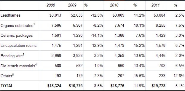
Packaging materials won’t have quite as good a year overall in 2010 as the overall sector, but it will be respectable with growth in the low teens both overall and in most segments, and could approach 15%, Tracy said — bookings through the half-year are already ahead of all billings through 2009. Top growth and best bounceback goes to encapsulation resins, and expect strong growth in organic substrates. Growth (in dollars) for bonder wire largely reflects the steep climb in the price of gold, though shipments also are growing steadily. Wire bond was 5.9% of 2009 shipments, twice what they were in 2008, and will reach 10% this year and 12%-13% in 2011.
For 2011 packaging materials also will see a slowdown to single-digit growth, though the "others" category — which includes things like wafer-level package dielectrics and solder balls — will stay in the low-teens. Note bonding wire lags the sector in 2011, barely eking out any growth at all (2%), just ahead of leadframes (although leadframe unit shipments have already surpassed pre-downturn levels).

(Source: SEMI)
1 Source is TechSearch International. Includes PBGA, PPGA, LGA, and CSP laminate substrates and flex BGA and CSP substrates
2 Assume gold value of $660/trz for 2007, $872/trz for 2008, $920 for 2009-2011 forecast period
3 Includes die attach film (tape) materials
4 Other includes solder balls and wafer level package dielectrics
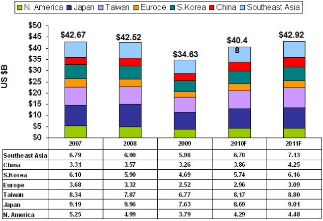
By region, Japan remains the largest installed capacity base, and there’s a lot of advanced packaging happening there too, Tracy pointed out. Taiwan also is strong due to its packaging houses and 300mm facilities. And three-quarters of China’s market are for packaging materials, as players move to advanced packaging technologies — that region actually grew in the lousy 2009 environment, Tracy pointed out.
 |
|
Materials forecast by region. (Source: SEMI) |

