(July 12, 2010) – Following are some of the highlights of the SEMICON West exhibit halls, open July 13-15 at the Moscone Center in San Francisco, CA. Products on display include TSV technology, ALD systems, vacuum and wafer transport tools, and more for semiconductor and package manufacturing.
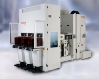 Multiwafer ALD system
The QXP-8300 multiwafer system is the next generation ALD product for dielectric and metal films. The applications comprise conformal high-<I>k</I> dielectrics for DRAM, eDRAM, MIM, logic, gate stack and flash IPD, as well as conformal electrode metals, i.e. metal electrodes and gate metal for DRAM, logic, and MIM. The tool offers a CoO proven by fab economics stating >$1M savings per year for 80k wafers start per month and >40% less precursor consumption compared to other ALD systems, the company says. Enabled by the TriJet vaporizer, the high-productivity system delivers excellent step coverage, i.e. 95% in >60:1 AR structures. Excellent WiW and WtW uniformity can be achieved since the unique Close Coupled Showerhead distributes the precursors homogeneously in short time. Due to its modular design the tool can be handled in a flexible way and is easy to maintain. No rotating parts ensures high system availability. Aixtron, #1907 (South)
High-aspect-ratio TSVs
AquiVia Fill is a high-purity, copper-plating chemistry designed for filling high-aspect- ratio through-silicon vias (TSVs) with diameters <5µm. These narrow vias help free up space on stacked chips and also improve signal integrity and system reliability. In combination with AquiVia XS, AquiVia Fill also extends chipmakers’ ability to shorten the metallization process, and slashes overall cost of ownership compared to traditional metallization processes. In contrast with current solutions based on complex and strongly acidic chemistries, AquiVia Fill is a mildly basic solution that does not attack or degrade the underlying films. It removes the need to electrically polarize the cathode, which can seriously degrade metal films due to excessive current density flowing through the small wafer area that receives first contact with the electrolytic solution. AquiVia Fill contains no chlorine, normally added to acidic solutions to boost the effect of additives. As a result, no CuCl crust forms on the anode, eliminating the risk of crust fragments detaching and depositing onto the wafer. This also reduces cost by eliminating the need for a filtering membrane between the wafer and the anode in legacy systems. Alchimer, #1811 (South)
Aligner wafer bonder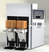
The FAB12 automated cassette-cassette aligner wafer bonder adds automated wafer handling to the unique benefits of the ground breaking AWB in-situ wafer bonding platform (align and bond in a single chamber) using robot systems from Brooks Automation to enable high-throughput processing for volume manufacture. Target applications include MEMS, IC, WLP, and 3D integration applications. The in-situ alignment tool maintains its industry leading throughput via simultaneous heating, pumping and alignment in a single bond chamber — no cluster tool required, minimizing footprint. It performs all standard wafer bonding processes with 1µm accuracy, as well as other unique processes such as; in-situ polymer/adhesive UV cure bonding and in-situ chemistry just before bonding contact. Wafer sizes: 150mm & 200mm (300mm ready). Applied Microengineering, #2631 (South)
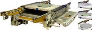 Wafer transport solution
DEK’s new wafer transport solution, available as an option on its Galaxy, Europa, and Horizon 01iX and 02iX print platforms, affords packaging specialists new levels of control, precision, and throughput for complex wafer level packaging processes. A specialized precision wafer pallet is central to the technology, as it allows for exceptional wafer flatness of wafers as thin as 75 microns and as large as 300mm in diameter. Movement of the loaded pallet into and out of the print platform is achieved through a next-generation rail system that has been engineered to provide outstanding stability, with precise control of speed, acceleration and positioning. The precision wafer pallet delivers superb flatness of the wafer to less than 10 microns within the critical process area, while the novel rail technology provides for stable movement control to facilitate excellent throughput and UPH. As part of a complete in-line system, DEK Wafer Transport Solution is capable of throughput rates of up to 60 wafers per hour and it enables a variety of applications including wafer bumping, DirEKt Ball Placement and wafer coatings, among others. DEK, #5251 (North)
Vacuum pump for semiconductor processing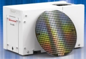
The iXL120, designed for load lock and other clean applications, offers peak pumping speed of 110m3/h, 22% faster than any other pump in its class (20 liter chamber), the company says. Average energy consumption (power at 700T exhaust pressure) is only 550W, one of the lowest in its class. It’s also small (450mm x 230mm x 280mm) and lightweight (59kg), so it can be mounted on the process tool or within the fib’s waffle floor. The pump incorporates oil lubricated precision bearings and timing gears to reduce vibration during pump operation, and it includes a zero nitrogen purge option (for processes that do not use corrosive gases to eliminate the need to provide nitrogen to the pump) as well as a nitrogen purge for use where there is a risk of corrosive gas carryover. Edwards, #2508 (South)
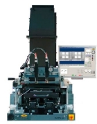 Semi-automated bond alignment
The EVG610 is a flexible desktop unit targeted for R&D and small-scale production needs in MEMS/MST markets. The EVG610 contains a precision alignment stage for optical bond alignment. Features include: a semi-automated alignment stage, fully motorized high resolution bottom side microscopes; IR alignment for inner substrate key alignment; and the company’s NanoAlign package for enhanced process capabilities. Substrate/wafer parameters are 2-3" and 100-150mm, 0.1-4mm thickness, and 4.4mm max. stack height. EV Group, #1225 (1225)
Cartridge filters
A new family of efficient cartridge filters specifically target filtration for ultrapure water (UPW) and de-ionized (DI) water used in the manufacture of semiconductors and silicon wafers. These filters offer 3x the flow rate of best-in-class filters without sacrificing particle retention, the company says, and can be easily substituted for filters in the field. They also can provide an alternative to ultrafiltration (UF) modules. The company cites current usage in fabs in the US and Asia. Gore, #2220 (South)
Reticle storage pod opener
The RSP opener is an economical solution to open/close standard reticle SMIF pods, vs. $20,000+ for auto RSP openers. In addition to being ergonomically designed and operator friendly, the unit includes a lid storage area and a mask pick holder; it also includes a handy mask pick holder. The product is ESD safe and constructed from cleanroom-compatible and chemical-resistant engineering plastics. H-Square, #907 (South)
Wafer backside coating for stacked die
The Ablestik WBC-8901UV material is designed to address the demanding requirements of multiple die stack applications for the memory market segment, including packages such as TSOPs, MCPs and FMCs (flash memory cards). The material offers a robust and cost-effective alternative to current film-based solutions for die stacking processes, reducing the total cost of ownership as compared to film by as much as 30%-50%, the company says. Die attach thickness can be adjusted based on specific manufacturing requirements and dicing tape is selected by the packaging firm. Film die attach materials are generally supplied in pre-determined thicknesses as a bundled product which incorporates the dicing tape. In combination with new spray coating technology, the material delivers a precise wafer coating as thin as 10µm with a total thickness variation across the wafer of +/-10% and remarkably low material waste of less than 20%. Wafers as thin as 50µm have been successfully processed using this method, the company says. Henkel, #721 (South)
SiGe-MEMS foundry, MPW service
IMEC has extended its CMORE offering with SiGe-MEMS foundry service and a multi-project wafer (MPW) service for universities and research centers, via its EUROPRACTICE IC service. Both services are based on a monolithically integrated SiGe MEMS baseline process and come with an extended design kit. The SiGe-MEMS technology is based on a MEMS-last approach, where the MEMS are processed after and on top of the CMOS circuits. It enables monolithic integration of CMOS and MEMS, integrating MEMS devices with the driving and readout electronics on the same die. Its flexible and modular approach allows application specific tuning and optimization — e.g., the thickness of the MEMS structural layer, which can vary between 300nm (for optical MEMS) and 4µm (for structural layer for gyroscopes or actuators). A 300nm-thick layer allows making optical MEMS, e.g. micromirrors. A first MPW run for initial prototyping is scheduled for the end of 2010; a second run with full capability and SiGe-MEMS devices on top of TSMC 0.18µm CMOS is scheduled for mid-2011. Imec, #1934 (South)
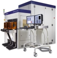 E-beam defect review, reticle inspection, overlay metrology
The eDR5210S is an updated version of the e-beam defect review and classification system released at last year’s SEMICON West, offering high resolution, stage accuracy, new algorithms, and unique access to proprietary data about mask orientation and defect characteristics from the company’s TeraFabHT reticle defect inspection system. A reticle defect review (RDR) mode simplifies and accelerates review of potential reticle-induced defect sites; the new version also introduces critical point inspection (CPI) mode, allowing a fab to monitor known ‘hot spots’.
The TeraFabHT reticle defect inspection system features improvements to its predecessor’s laser, sensor, optical path, and signal processing algorithms, including the company’s patented STARlight mode that enable increased detection sensitivity and throughput. The new tool also allows inspection of single-die and multi-product masks, leading-edge mask types using novel materials (such as OMOG) and designs employing unusually small OPC features.
The Archer 300 LCM provides high-performance overlay measurement capability for 2Xnm logic and 1Xnm half-pitch memory devices. Improvements to the optical subsystems deliver unsurpassed precision, better measurement repeatability, and faster measurement speed than the Archer 200. New in-field overlay metrology capability and support of a smaller metrology target allows lithographers to take more measurements across the wafer, and supports characterization of overlay error for double patterning and other advanced process technologies. It is upgradeable from existing Archer metrology tools.
KLA-Tencor also has a new client/server service model, KlearPoint, with a customized data interface to the company’s inspection and metrology tools to collect operational and tool parameter data in real time.
KlearPoint is a new service model that utilizes KLA-Tencor experts to proactively manage tool performance through real-time tool monitoring. KlearPoint can be added to service agreements to improve tool performance and productivity for customers worldwide. The service is aimed at maximizing Overall Equipment Effectiveness (OEE) by increasing uptime and recipe success, reducing lost-time due to interrupts and enabling a more predictive and preventive service model. The KlearPoint client-server system resides within the customer site and connects to KLA-Tencor inspection and metrology tools using a customized data interface that collects operational and tool parameter data in real time. With this data, which is obtained and analyzed using algorithms specifically developed for this application, KLA-Tencor experts can conduct drill-down analyses and help determine the root causes of problems—providing a proactive service delivery model that results in improved tool performance and productivity. KlearPoint is installed at multiple customer sites throughout the world. KLA-Tencor Corporation (NASDAQ: KLAC), #1947 (South)
Ultrasonic DSP flowmeter
The LeviFlow ultrapure ultrasonic flowmeter is designed for non invasive high-precision flow measurements of high purity fluids from 1ml to 80l/min. Features include high accuracy (1% of reading) and repeatability (≤ 0.5%), improved bubble robustness (a digital signal processor handles the sensor signals), and high-precision flow control with the company’s MagLevPump. For high-volume applications a multi-channel converter is available, which processes 6 sensors with one single converter. Levitronix, #2408 (South)
Residual gas analyzers
The Microvision 2 and e-Vision 2 Web-enabled residual gas analyzers offer greater stability and reliability in e-diagnostic, process monitoring and general vacuum trouble-shooting applications, building on the company’s Microvision Plus, e-Vision and Vision 1000 product lines. The platform uses robust proprietary technology for data acquisition, with industry standard technology for communication and control. Improved I/O capacities, higher data quality, and enhanced speed and accuracy enable capture of a greater number of process excursions and more accurate alarm decisions with fewer false positives. They are available for new or established installs alongside other instruments in the MKS range of process RGAs and gauges. MKS Instruments, #5356 (South)
Single-axis bearing stages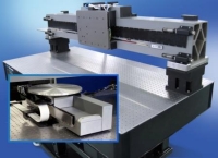
The SinguLYS family of modular bearing stages target single-axis, split XY, and gantry applications. The S-370 stage made from SiC ceramic components can be used in tight spaces (e.g. mechanical bearing designs), and features integrated pressure-vacuum air bearings. It’s ideal for very high-duty cycles requiring low angular deviation and tight velocity regulation. The B-1200 bridge has a proprietary ceramic beam to replace steel or granite-based designs for improving acceleration and decreasing settling times. It accommodates high (10kg) cantilevered payloads with 2.5G acceleration and, unlike stages using mechanical bearings, minimizes contamination to the substrate below. Applications include Gen 8-11 flat panel display inspection, thin film photovoltaic scribing, and wafer processing. Newport, #1807 (South)
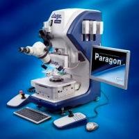 Bond tester
The 4000Plus can perform a wide range of shear and pull applications as well as new push functionality up to 50kg, suitable for the full spectrum of traditional bond tests as well as emerging test applications including ribbon pull, new hot bump pull and fatigue. A unique anti-backlash system aids the setting and control of step back. The system is available with a range of XY stages, with a 160mm XY stage as standard and an image capture system for advanced analysis that is quick to set-up to aid faster testing; it also has an extended working envelope of 200mm for testing oversize parts. The system utilizes Nordson DAGE’s Paragon software that offers functionality including semi-automatic test routines and automatic GR&R calculation. Nordson Dage, #5947 (North)
Flux jetting system
The Spectrum S-930N series selective flux jetting systems for low-viscosity flux and phase-change high-tax fluxes enable thin flux coatings as low as 5microns; selective flux jetting provides 0.5-1.0mm edge definition to minimize flux residue and overspray. Fluidmove software controls the amount of flux jetted to accommodate flip chips of varying bump heights. A dual lane configuration is available for high-volume production. The company’s MH-900 series loaders/unloaders can be added for inline production or in a work-cell configuration with a same-side load/unloader. Nordson Asymtek, #5947 (North)
Wafer handler
The Olympus AL120 wafer handling system, its newest generation, delivers the renowned performance and reliability for which Olympus microelectronics products are known. The AL120 system transfers wafers with thicknesses down to 90 micrometers to meet the demands of thin-wafer manufacturing. The new system offers 360-degree rotation, for full macro examination of the wafer’s back surface and edges. User friendly and recipe driven, it can be programmed for different configurations, including specific cassette types, wafer specifications and transfer speeds. Quick push-button recipe selection allows the operator to load different products instantly. The AL120 wafer handler accepts wafers that are 100-200mm in diameter. It can be adapted for smaller-diameter wafers and used with non-Olympus microscope models on a custom basis. The AL120 wafer handler is fully compliant with international Reduction of Hazardous Substances (RoHS) standards. Olympus America Inc.’s Scientific Equipment Group – Industrial Microscopes. #6047 (North)
IR thermometer to measure annealing temps
The OS1592 infrared fiber-optic thermometer/transmitter features a local display and two isolated analog outputs that indicate current plus min, max, or differential temperatures — up to 2482 degrees Celsius with 1% reading accuracy. A built-in relay, alarm LED, and a 4-position programmable keypad adjust emissivity (0.05 to 1.00) and high & low alarm set points. The system is well-suited for both hard-to-reach small areas and polymer bolt applications in semiconductor manufacturing to monitor the temperature of the wafer during electrical test and other manufacturing processes, as well as metal annealing to monitor the temperature of annealing process. Omega Engineering, #5778 (North)
Gas purifiers for CDA and HBr
The latest additions to the Areskleen media for the purification of lithography clean dry air (CDA) and hydrogen bromide (HBr) gases. The CDAP material removes moisture (H2O), hydrocarbons, refractory compounds, acidic and basic gases in CDA to or below the levels specified in the 2009 ITRS. The HBRP material removes H2O to <50 parts per billion (ppb) in HBr gas. Both materials are available in the company’s standard Gaskleen Purifier assemblies with flow rates up to 1,000 standard liters per minute (slpm). Assemblies include integral 3nm or 0.4µm particle filters. Pall, #1721 (South)
Magnetically levitated turbopumps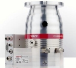
The HiPace M series offer high pumping speeds (300 l/s, 700 l/s and 800 l/s) and high compression ratios for all gases, optimized to run in all orientations with a low vibration signature. An advanced rotor design provides unlimited rotor service life and dependable operation. These pumps are rated Protection Class IP54 for harsh industrial environments. An intrinsically low dynamic magnetic field does not interfere with even the most sensitive equipment. An integrated electronic drive unit reduces the need for cabling and cable failure. Power consumption and run-up time also have been reduced. An optional sealing gas connection safeguards against particulate buildup and oxidizing gases. Pfeiffer Vacuum, #532 (South)
Reducing waste in wafer processing
The CoreTegral framework helps manufacturing facilities develop an open, maintainable system for centralized integration and automation of process equipment in an entire facility, irrespective of the equipment’s age or manufacturer. Designed to be flexible and extensible — and maintained by IT professionals, not process engineers — it is built on industry-standard C# within the .NET environment, utilising Microsoft SQL Server as the detailed automation data cache. Savantech, #1813 (South)
Test for power semiconductors
The Comptest MX Platform, already offered as a general purpose SoC & SiP test platform, has been enhanced with specific instrumentation for the production test of power devices, to force high current/voltage while performing multi-site test, with the additional possibility to integrate test and automation. It can perform the test at wafer or package level, combining static and dynamic test capabilities. Features include automatic spike detection to avoid damage on the device, and embedded alarms on high-voltage and high-current modules (e.g. over temperature, over current, floating, Kelvin, etc). Also new: the PMTC 100 test cell for automated handling, contacting and testing of IGBT and semiconductor power modules. SPEA, #5577 (North)
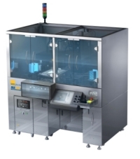 Mask aligner for HB-LEDs; semiautomatic MEMS bonding
The MA100e mask aligner offers a dedicated lithography solution for manufacturing high-brightness light emitting diodes (HB-LEDs), as well as other compound semiconductors, such as power devices or RF-MEMS. It processes wafers up to 4in. with throughput up to 145 wafers per hour (215 wph first mask) with reduced cycle times. High-intensity exposure optics and pre-alignment options shorten process time while functionalities like proximity exposure for high resolution down to 0.7µm maximize yield and cost-efficiency. It can be equipped with an innovative multisize toolset that minimizes the time required for wafer size changeover, leading to exceptional process scalability. Alignment microscope, camera system and advanced alignment software of the MA100e Gen2 are tailored to the specific requirements of HB-LED manufacturing and offer excellent contrast even on transparent and textured wafers. Targets can be found even if the surface background changes one each wafer.
The semi-automatic CB200M features bond forces up to 90kN and temperatures to 500°C, ideal for advanced MEMS, 3D stacking and LED bonding applications, supporting advanced eutectic, fusion and metal fusion bond processes. For full production needs, a 200M transfer station to load the wafers into the bond module can be docked onto a CBC200 production bond cluster. Pressurized gas applies force instead of hydraulic fluids to keep the process and clean room free of contamination. Unique vacuum isolation layers focus heat conduction pathways and enable rapid heating (30°C/min) and cooling times (20°C/min) and ensure excellent temperature uniformity (±1%). Suss Microtec, #1707 (South)
Ammonia gas analyzer for HB-LEDs
The Aloha ammonia analyzer utilizing cavity ring-down spectroscopy is designed and manufactured exclusively for HB LED-related applications. Users can measure moisture in ammonia and inerts. There are no off-line periodic sensor maintenance procedures, no span calibrations, no purifier replacement and no pump rebuilds required. It can detect down to 10ppb with 5ppb sensitivity and 4% of reading accuracy (+/- 5ppb), for gas flow rate up to 1000 sccm and up to 60°C. Tiger Optics, #1431 (South)
Single-touchdown full-wafer DRAM probe card
The 1Td300 full-wafer probe card offers single-touchdown, high-volume testing of advanced DRAM memory devices, capable of highly parallel testing of 300mm or 200mm wafers. It can test an entire 300mm wafer with an industry-low 2g of force per probe, less than half that of comparable products. Touchdown, #5847 (North)
Plasma strip and MEMS release
The ENVIRO- 1Xa advanced plasma resist strip system, designed for non-300mm fabs, can handle the complete line of wafer sizes (4-8-inch), capable of high-speed photo resist removal at more than 10µ/min with excellent repeatability and high reliability. It can also function as a MEMS device release tool for removing sacrificial film layers. Features include a choice of plasma sources (high-rate downstream MW, or RIE), >10µ/min ash-rate (high-rate downstream plasma source), high throughput, auto endpoint detection, dual cassette loading, compact footprint, GUI and touch screen; and the system is EU-RoHS compliant. Applications include resist strip for LED and power device manufacturing, high dose implanted resist removal, bulk resist strip, descum, and MEMS sacrificial layer removal. Ulvac, #1321 (South)
Visit the SEMICON West center for more of the latest news from the show: http://www.electroiq.com/index/Semiconductors/semiconwest2010.html

